By Mark Tawfik
Overview: Protecting ICs from costly ESD and latch-up failures
Electrostatic discharge (ESD) events cost the semiconductor industry an estimated $8 billion annually in lost productivity, warranty claims and product failures [1].
Ensuring the robust protection of integrated circuits (ICs) against various electrical phenomena, is a critical and often complex task in modern electronic design automation (EDA) verification, with even minor ESD incidents capable of triggering catastrophic latch-up events that can permanently damage sensitive components Preventing latch-up— a parasitic condition that can lead to device failure—is paramount, with guard rings playing a crucial role in its mitigation. ESD mitigation requires a multifaceted approach centered around robust guard ring implementation and comprehensive verification.
Different IC design companies employ diverse protection methodologies, design flows and verification tools, leading to potential inconsistencies. To establish a consistent, comprehensive and efficient verification flow for critical reliability aspects, the ESD Association (ESDA) provides recommended compliance checks. The Calibre PERC reliability platform from Siemens Digital Industries Software offers a suite of easy-to-use, pre-coded packaged checks for latch-up and the effective implementation of guard rings. This allows design companies to perform fast and efficient verification of ESD protections without the need to develop and maintain their own custom checks. By streamlining the design process. Calibre PERC helps design teams enhance overall device reliability. [4]
The pervasive threat of electrostatic discharge (ESD)
Electrostatic Discharge (ESD) is a rapid, uncontrolled transfer of static electricity between two objects at different electrical potentials. This static charge can accumulate on various surfaces or even human bodies through friction or induction. When a charged object comes into proximity or direct contact with a less charged or grounded object, the stored electrical energy discharges instantaneously, often generating thousands of volts and significant current pulses lasting only nanoseconds.
While static shocks are familiar phenomenon, in advanced manufacturing and electronic environments, ESD events pose a severe and costly threat. Even minor discharges can inflict critical damage on highly sensitive IC components. This damage can manifest in several ways:
- Immediate catastrophic failure, where the device ceases to function
- Latent damage, which may not cause immediate malfunction but degrades performance over time, leading to premature field failures
- Parametric shifts, altering device characteristics without complete failure
Common failure mechanisms include gate oxide breakdown due to high electric fields, junction damage from excessive current and metallization burnout caused by localized heating. Such incidents directly translate into reduced manufacturing yields, increased warranty claims, costly product recalls, and significant financial losses for semiconductor companies. [3,6]
The challenges of latch-up
Complementing ESD as a paramount reliability concern in IC design is the phenomenon of latch-up. Latch-up refers to the inadvertent triggering of a parasitic Silicon Controlled Rectifier (SCR) structure inherent within the bulk CMOS (Complementary Metal-Oxide-Semiconductor) process. This parasitic SCR is formed by the interaction of adjacent p-n junctions, specifically the p-well, n-well, and substrate, creating a parasitic NPN-PNP bipolar transistor pair.
Under certain conditions, such as voltage transients, overvoltage events or current injection into input/output (I/O) pins, this parasitic SCR can be triggered into a low-impedance, high-current state. Once triggered, a positive feedback loop is established between the parasitic bipolar transistors, sustaining a large, uncontrolled current flow between the power supply and ground.
This sustained high current draw can lead to several severe consequences:
- Complete functional failure of the circuit
- Thermal runaway due to excessive heat generation
- Permanent physical damage to the device (e.g., metal trace burnout, junction degradation)
- Collapse of the system’s power supply.
Latch-up events can be initiated by various factors, including I/O overvoltage, power supply transients, or even an ESD event that injects sufficient current to trigger the parasitic structure. Once latch-up occurs, it is challenging to mitigate and typically requires the device to be powered off or physically reset to restore normal operation, highlighting the critical need for robust prevention mechanisms during the design phase.

Latch-up prevention techniques
Latch-up prevention is a critical aspect of integrated circuit (IC) design, employing a multifaceted approach to mitigate the risks associated with parasitic current flow.
A cornerstone of latch-up prevention is the careful optimization of the IC layout. This involves strategic placement and spacing of components to inherently suppress the formation of parasitic thyristors—the PNPN structures responsible for latch-up. Central to this strategy is the implementation of guard rings—heavily doped regions strategically placed around sensitive transistors and circuit blocks.
Guard rings serve two key functions:
- They absorb minority carriers, preventing them from reaching and activating the parasitic bipolar transistors that constitute the latch-up path.
- They act as physical barriers, diverting excess current away from vulnerable areas and providing electrical isolation between different regions of the IC. [2]
This helps minimize unwanted interactions, maintain signal integrity, and enhance overall IC robustness by containing and dissipating potential trigger currents.
Beyond guard rings, other critical latch-up prevention techniques include:
- Maintaining optimal spacing between p-wells and n-wells to physically increase the resistance of parasitic paths
- Employing precise biasing techniques to control the substrate potential and keep parasitic elements in a non-conductive state [2]
The integration of robust ESD protection circuits also plays an indirect role by clamping and shunting transient overvoltages and overcurrents that could otherwise trigger latch-up.
Finally, advanced semiconductor processing techniques, such as using Silicon-On-Insulator (SOI) technology, significantly enhance latch-up immunity by providing intrinsic dielectric isolation between devices, dramatically reducing parasitic interactions and virtually eliminating bulk latch-up paths. Similarly, precise optimization of doping concentrations and profiles within the silicon substrate allows for better control over the electrical characteristics of parasitic elements, making them less prone to activation.
By integrating these comprehensive design and process techniques, IC designers can significantly minimize the risk of latch-up events, ensuring the reliable performance of integrated circuits across a wide spectrum of applications.
ESDA’s reliability guidelines for IC designers
ESD Association (ESDA) is a leading industry association dedicated to advancing the understanding, theory and practice of electrostatic discharge (ESD) avoidance. Recognizing the critical impact of ESD on IC reliability, the ESDA develops and publishes comprehensive guidelines, standards, and technical reports. These resources provide a standardized framework of design rules and corresponding compliance checks, serving as indispensable tools for both the electronic design automation (EDA) industry and the ESD design community. Their primary aim is to empower IC design teams to proactively protect their layouts from the damaging effects of ESD events and ensure overall device robustness. [2,3]
ESDA latch-up guard rings checks
Building upon these industry standards, EDA vendors strive to develop advanced verification solutions to address these critical reliability concerns. An example of such a solution is the Calibre PERC reliability platform from Siemens Digital Industries Software. This platform is designed to perform a range of complex design verification checks and can be integrated into existing design flows. It supports verification at various levels, including cell, block, and full-chip, and facilitates the implementation of reliability checks using both standard rules provided by foundries and custom rules defined by design teams.[5]
To effectively address these pervasive reliability threats, all potential sources of ESD and latch-up events within an IC design must be thoroughly evaluated and verified. In this context, Calibre PERC specifically addresses latch-up prevention by incorporating latch-up guard rings packaged check. This check support various critical verification aspects, encompassing 14 distinct checks, shown in figure 2, further categorized into five key areas:
- Check guard ring existence
- Check guard ring width
- Check max spacing between Guard rings
- Check victims in aggressor’s danger zone
- Check guard rings connectivity

By enabling the early identification and resolution of potential latch-up issues during the design phase, these advanced checks significantly reduce time-to-market for microelectronics designers and producers. This proactive approach prevents costly post-production failures, thereby improving yield, enhancing device reliability and compliance, minimizing field failures, and streamlining design iterations for faster, more efficient product development.
Guard rings existence checks
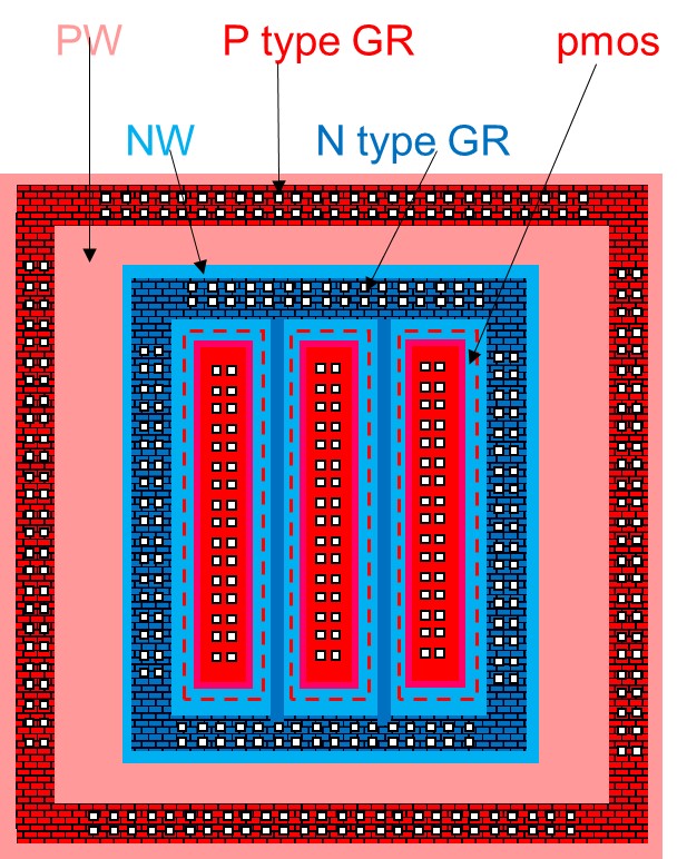
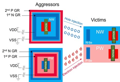
Verifying the existence of guard rings in a design is critical because these structures serve as a primary protective measure against latch-up phenomena in CMOS and mixed-signal circuits. Guard rings act as barriers that prevent injected minority carriers—generated during transient events, such as voltage spikes or substrate noise—from reaching sensitive device junctions and triggering parasitic thyristor paths. Without the presence of guard rings, the circuit is left exposed to increased risk of latch-up, which can lead to excessive current flow, functional failure, or even permanent damage. Therefore, confirming that guard rings are present wherever needed ensures that the foundational layer of latch-up protection is robustly in place. These rules verify the existence of the four types of guard rings (GR) illustrated in figure 3. The checks ensure that:
- 1st P type GR must enclose N+ aggressor
- 1st N type GR must enclose P+ aggressor
- 2nd P type GR must enclose P+ aggressor
- 2nd N type GR must enclose N+ aggressor

Guard rings’ width checks
The width of a guard ring strongly influences its ability to intercept and collect stray charge carriers before they reach vulnerable regions of the integrated circuit. If the guard ring is too narrow, it may not fully encompass the region it is supposed to protect, allowing some injected carriers to bypass the barrier and trigger latch-up. Adequate ring width ensures a greater area for carrier collection and improves the effectiveness of the ring as a protective shield. By rigorously checking that guard ring widths adhere to design rules and process requirements, engineers can significantly reduce the risk of latch-up and enhance the reliability and longevity of the chip.
The checks cover:
- Width of P type Guard rings
- Width of N type Guard rings
Guard rings spacing checks
The spacing between adjacent guard rings and aggressors plays a vital role in maintaining continuous protection across the chip. If guard rings are spaced too far apart, gaps appear in the protective network, leaving certain regions susceptible to carrier migration and latch-up initiation. Carefully monitoring and enforcing the maximum allowable spacing ensures full coverage of critical areas, creating a seamless defense system that blocks potential latch-up pathways. These checks help eliminate weak points in the design and boosts overall device robustness by maintaining the integrity of the guard ring network.
The checks cover:
- max spacing between P type aggressor and 1st N type guard ring
- max spacing between 1st N type guard ring and 2nd P type guard ring
- max spacing between N type aggressor and 1st P type guard ring
- max spacing between 1st P type guard ring and 2nd N type guard ring
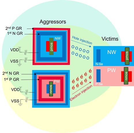
Aggressor’s danger zone checks
Sensitive components, referred to as “victims,” located near regions with high-current drive or frequent switching activities—known as “aggressors”—are at particular risk for latch-up. In these danger zones, increased noise and carrier injection elevate the probability of parasitic conduction. By identifying and analyzing potential victims within these aggressive regions, engineers can prioritize additional guard ring protection and optimize layout strategies to mitigate risk. This targeted approach greatly enhances the effectiveness of latch-up prevention by focusing resources and attention on the most vulnerable spots within the circuit by check the non-protected victims in an aggressor’s danger zone, where the danger zone is marked by drawing a radius around the aggressors, as illustrated in figure 4.
The checks cover:
- max spacing between P type aggressor and 1st N type guard ring
- max spacing between 1st N type guard ring and 2nd P type guard

Guard rings connectivity checks
Proper guard ring connectivity is essential to ensure that these protective structures are electrically functional and capable of steering excess charge to a safe potential, typically ground or VSS. If guard rings are not correctly tied to the designated bias, their ability to collect and divert injected carriers is compromised, undermining latch-up prevention. Connectivity checks involve confirming robust electrical contact and continuity through all relevant routes and layers. Ensuring reliable guard ring connections fortifies the overall defense against latch-up, preserving the operational integrity and safety of the integrated circuit throughout its lifecycle.
The checks cover:
- N type Guard rings not connected to VDD.
- P type Guard rings not connected to VSS
Simplifying ESD check implementation with packaged checks
However, the mere availability of ESDA checks is only the initial step; designers often face challenges in effectively setting up and executing these checks within their specific environments. To significantly simplify and standardize the application of ESDA guidelines, Electronic Design Automation (EDA) companies, such as Siemens EDA, encapsulate these checks into pre-coded, packaged solutions. These readily deployable checks can be seamlessly integrated into a design team’s existing reliability verification flow, eliminating the need for manually coded checks and the associated complexities. Designers can embed these Calibre PERC reliability checks directly into their current design flows, leveraging the integrated Calibre platform for comprehensive cell, block, and full-chip verification. This approach, which brings together rules coded in both standard verification rule format (SVRF) and Tcl-based Tcl verification format (TVF), provides designers with the flexibility and adaptability needed to meet evolving design requirements while ensuring compatibility across all major foundries. Furthermore, to provide consistent and accurate coverage of the ESDA rules, the Calibre PERC platform includes packaged checks tailored for each of the four ESD coverage categories, allowing designers to invoke them with either default parameters or customized modifications.[4]
Results debugging
Design teams can run any combination of Calibre PERC latch-up guard rings packaged checks, then analyze and debug the results using the Calibre RVE results viewer, as shown in figure 5.

These checks are accompanied by a comprehensive debug database, designed to facilitate the rapid identification and resolution of violations. Designers can effectively pinpoint issues by highlighting the results and debugging layers directly within the Calibre RVE. This visual approach streamlines the debugging process, as illustrated in the accompanying figure 6.[4]

Conclusion: Packaged ESD checks improve reliability and time-to-market
Electrostatic discharge (ESD) and latch-up verification using Electronic Design Automation (EDA) tools presents a significant challenge due to the varied protection approaches and diverse verification tools employed across integrated circuit (IC) companies. This paper has provided an overview of latch-up events, detailed effective prevention techniques, and illustrated how specific verification checks integrate into typical IC product and IP development flows. Focusing on the critical role of guard rings in robust latch-up protection, we introduced the Calibre PERC ESDA latch-up packaged checks. This innovative solution offers a user-friendly and efficient method to apply ESDA guidelines swiftly and accurately, enabling comprehensive latch-up verification across any technology node. By leveraging these Calibre PERC packaged ESDA latch-up checks, designers can achieve rapid and precise reliability verification, thereby significantly reducing time-to-market. [3]
References
- [1] Semico Research Corporation. “The Cost of ESD: $8 Billion Annually for the Semiconductor Industry.” Semico Insights, 2018. https://semico.com/content/cost-esd-8-billion-annually-semiconductor-industry
- EDA Tool Working Group (2014), “ESD Electronic Design Automation Checks (ESD TR18.0-01-14)”, New York: Electrostatic Discharge Association, January 2015, https://www.esda.org/store/standards/product/4/esd-tr18-0-01-14
- Mark Tawfik “Ensuring ESD Protection Verification with Industry-standards checks,” Siemens Digital Industries Software. December, 2022. https://semiengineering.com/ensuring-esd-protection-verification-with-industry-standard-checks/
- Hossam Sarhan “Configurable, easy-to-use, packaged reliability checks,” Siemens Digital Industries Software. March, 2019. https://resources.sw.siemens.com/en-US/white-paperconfigurable-easy-to-use-packaged-reliability-checks
- Calibre PERC reliability platform, Siemens Digital Industries Software. Sept. 2017. https://resources.sw.siemens.com/en-US/fact-sheet-calibre-perc
- Derong Yan. “Ensuring robust ESD protection in IC designs” Siemens Digital Industries Software. Oct. 2017. https://resources.sw.siemens.com/en-US/white-paper-ensuring-robust-esd-protection-in-ic-designs
Also Read:
Something New in Analog Test Automation
Tessent MemoryBIST Expands to Include NVRAM
Smart Verification for Complex UCIe Multi-Die Architectures
Share this post via:


Comments
There are no comments yet.
You must register or log in to view/post comments.