By Zameer Mohammed
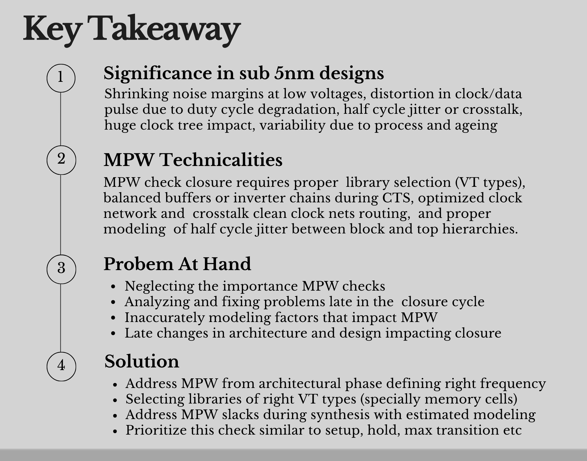
This article claims to provide clear key insights of Min Pulse Width (MPW) timing signoff check, proactive closure strategies for faster time-to-market, and effective methods to prevent silicon failures.
Min Pulse Width (MPW) check for timing signoff has become an important design constraint at the sub-5nm technology node. Recently, there have been reports from multiple companies of silicon failures associated with MPW. These failures point to inadequate modeling of design margins related to MPW, gaps in timing signoff verification process and underestimation of the issue’s importance. It is essential to recognize and address this challenge to prevent delays in bringing products to market and avoid costly silicon failures.
These issues indicate limited modeling of design margins related to MPW, gaps in the timing signoff verification process, and an underestimation of the significance of the issue.
(1) Introduction
What is Min Pulse Width (MPW) timing check?
Min Pulse Width (MPW) for a logical cell is shortest, non-zero finite duration of a logic “high” or “low” signal at the input that can be correctly propagated and processed by the gate at its output as a valid logical transition. MPW requirement acts as low pass filter for rejection of unwanted glitch and transient noise by effectively filtering them.
Impact of MPW Failure
If the input stimulus is narrower than MPW specification, it might be filtered out entirely (absorbed, no change at the output) or attenuated below threshold producing an invalid transition at the output (glitch or runt pulse), leading to logic errors and incorrect circuit behavior besides damaging internal gate circuits due to stress. Also possible at the output is an unstable “metastable state” that can persist for an indeterminate amount of time leading to delays and potential circuit failure.
Relevance to STA Signoff
- Transistor symmetry mismatches within gate are increasingly significant at sub 5nm
- Crosstalk and wire induced slew degradation affect MPW and signal quality
- Higher clock speeds heighten metastability issues due to MPW failures
- Elevated temperatures reduce transistor switching speed, impacting MPW
- High activity and current density in clock nets may degrade performance over time
A robust STA signoff for Min Pulse Width checks should account for accurate waveform propagation, crosstalk and On-Chip-Variation (OCV) and other margins and derates.
Target design elements with MPW check
- Clock pins of flip-flops (high AND low)
- Enable pins of latches (high OR low)
- Preset and clear pins of flip flops (high OR low)
- Clock pins of memory (high AND low)
- Memory (high OR low) write enable, chip select, and output enable
- Custom IP clock/reset pins
- Additional user MPW constraints on source synchronous or output clocks of a design
Combinational gates do not have min pulse width check, as they have lack memory and transmit all input signal when the input is held longer than the intrinsic gate delay.
Why MPW must be a finite value?
Temporal resolution limit for MPW is due to intrinsic physical and electrical limitations in how the logic gates operate. Logic gates are modeled as discrete logic and governed by continuous-time analog dynamics where internal RC networks & transistor drive strengths act as low pass filters that prevent arbitrary short pulses from producing full logic level swings. A certain amount of switching time is needed to detect an input level change, perform internal charging/discharging capacitances, and propagate the change to its outputs. In summary, for the output to transition to a new stable state, input must be held at new state for duration at-least the propagation delay.
(2) MPW & Duty Cycle Degradation
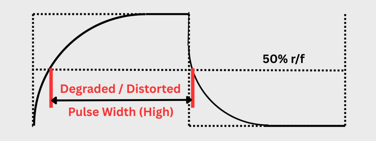
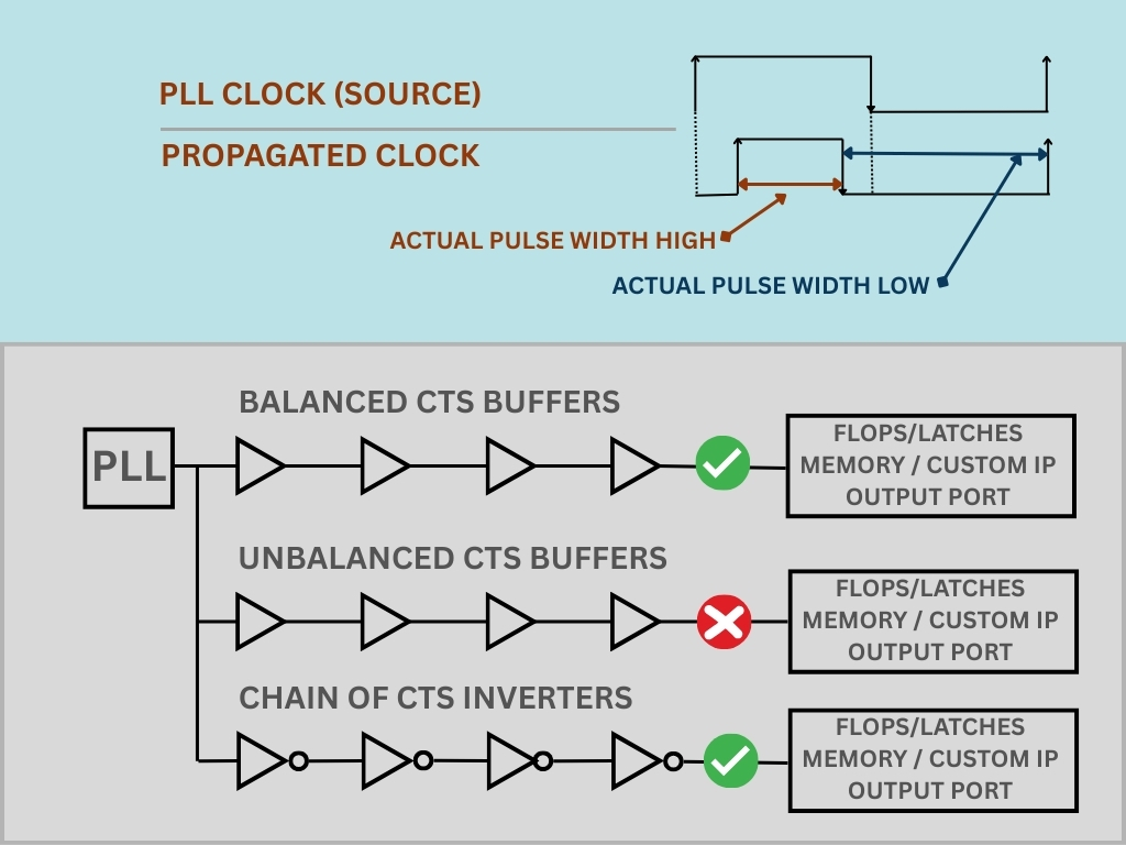
Clock waveform quality declines throughout the network due to “duty cycle degradation,” which lowers high or low pulse integrity. Major causes include:
.01 Low Pass Filter Effect – The clock or logic network functions as a series of RC filters, progressively reducing signal pulse width.
.02 Non-symmetrical Rise/Fall Delays – Real CMOS circuits often have uneven pull-up and pull-down strengths making rising edges propagate differently from falling edges and degrading the duty cycle over the network. This effect is modeled as process sigma variation in standard cell library. This cannot be credited as part of Common Path Pessimism Removal delay unlike nominal delays modeled by mean portion of standard cell delay.
.03 Loading Effect – Greater load in clock or logic stages slows edge transitions, increasing the time to cross the threshold and raising the minimum pulse width requirement.
.04 PVT Dependence – Low voltage (V) and high temperature (T) equates to weaker drive strength and smaller currents and makes the pulse width degradation worse.
.05 VT (channel length, threshold voltage) affects MPW requirements; shorter VT channel lengths need higher MPW requirement due to greater process variation, delay imbalance and short-channel effects.
.06 On Chip Variation Derates – Adjustments associated with process, voltage, temperature, distance based SOCV, wire, aging and radiation.
.07 Modeling Effects – Half Cycle Jitter narrows the effective clock pulse shape by altering its shape.
,08 Crosstalk – Any effective coupling on logical network will negatively impact each of rise/fall paths (both directions) and this incremental delay due to crosstalk does not cancel out as part of Common Path Pessimism Removal.
(3) MPW Slack Calculation
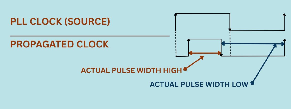
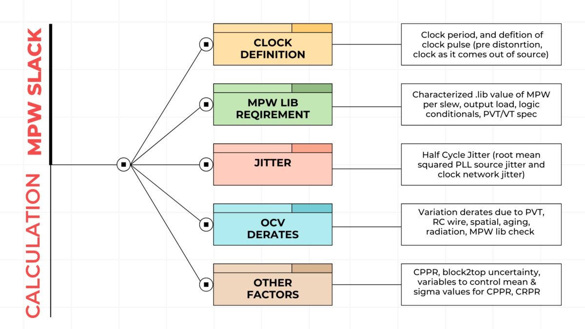
MPW Slack (High Pulse) = Propagated Fall Edge (minimum) – Propagated Previous Rise Edge (maximum) – (Cumulative Half Cycle Jitter) – LIB MPW Spec – Flat Uncertainty + CPPR Credit
MPW Slack (Low Pulse) = Propagated Rise Edge (minimum) – Propagated Previous Fall Edge (maximum) – (Cumulative Half Cycle Jitter) – LIB MPW Spec – Flat Uncertainty + CPPR Credit
Note: derates impact all delays compounded to cells/nets and not represented by a single value in equation and crosstalk delays not credited as part of CPPR credit for rise/fall and they impact slack negatively).
The first edge (rise for MPW high) is calculated as late as possible, and second edge (fall for MPW high) is calculated as early as possible. Since these semantics match setup style checks, MPW is normally reported in setup views. Doing these checks in hold views can produce optimistic results.
MPW is not reported on data and asynchronous pins. However dummy clock can be created on driver port to force tools to report MPW.
(4) MPW .lib (liberty format) syntax
A sincere attempt is made below to show the MPW spec as defined in library files (.lib liberty format) and brief explanation to interpret the same.
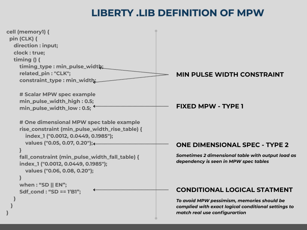
How MPW is characterized?
Minimum pulse width (MPW) characterization involves measuring the shortest pulse width for all clock and asynchronous set/reset pins. MPW is determined through a binary search, shrinking the pulse width until a failure criterion is met, i.e. either the output fails to switch, or the output peak voltage does not reach the required glitch-peak. This can be done by transistor level sub circuit extraction, applying input waveform of varying widths and sweeping across supply voltage, process corners and temperatures and measuring output.
During ETM generation, the MPW defined at the CK pin of the registers are transferred to the clock source port in ETM.
(5) How to Analyze & Fix MPW Violations
MPW timing should be verified thoroughly, regardless of whether the worst reported slack is positive. Additionally, MPW slack can be custom reported to a predefined list of endpoints (critical memories, output ports, custom IP pins etc.) to ensure comprehensive reporting without omissions.
Root Cause Analysis & Strategy To Avoid/Fix Violations
- Accurate clock definition including waveform as it reaches MPW check endpoint.
Sometimes clocks are gated/regenerated and clock waveform modified before reaching destination pins. For slower L2/L3 memories where latency is less critical, the final clock may be set as Multicycle or Extended Pulse to relax MPW & Min Period constraint. Ensure generated clocks are accurately defined at right generated point without over-constraining MPW check. Hacking reports or waiving violations after being reported to compensate for inaccurate clock waveform definition is not efficient due to postprocessing effort and possibility of making errors.
- Realistic MPW spec value as set by library or user definition
MPW high required value must be less than the clock pulse width high definition, besides accounting for half cycle jitter, duty cycle degradation, and derates. Otherwise, this might indicate improper memory configuration case analysis settings during memory compilation or linking of incorrect libraries. If so, review the conditional statements for the MPW spec in the .lib file and check proper library usage.
Also check to make sure right VT flavor of memory selected. Sometimes, lower VT memory must be selected at the expense of power to meet strict MPW spec.
- Accurate half cycle jitter modeling, a function of pll jitter and clock network jitter components
During MPW signoff, select PLL jitter according to the appropriate PVT corner rather than using general approximations or a uniform specification for all timing corners. Next, ensure that the jitter resulting from clock propagation between the PLL source and its destination is thoroughly and accurately calculated (how CTS jitter is specified is beyond the scope of this article, but there is a structured way to generate this spec based on input slew, cell VT types, statistical foundry models and Monte-Carlo simulations). The final jitter should be determined either by conservatively summing the PLL jitter with the CTS network jitter or by employing RMS method (recommended) for greater accuracy. Additionally, it is important to confirm that the assumptions regarding top-level clock tree depth are correctly represented at the block level, thereby preventing any discrepancies at the top level.
- Check accuracy of derates and margins applied
In MPW signoff mode, derates for aging, wire/RC, radiation, voltage, temperature and process (from library cell delay mean) are generally skipped, as source and destination clocks trace the exact path; only process derate sigma is excluded from CPPR credit if N and P device variation is modeled as process sigma component of cell delay. In this case, statistical variation is occurring at different edges and cannot assumed to be nullifying each other. Tools offer variables to control mean and sigma credit percentage, with some designers adding extra pessimism by not using CPPR credit. Not taking any CPPR credit is also very pessimistic. Always follow company guidelines based on thoroughly reviewed timing signoff spec. Usually this specification is defined by circuit and library teams based on earlier silicon feedback. Additional uncertainty may be used for min pulse width checks to safeguard against silicon failures. Setting proper derates is both an art and science balancing yield and time-to-market. Test chips can help refine derate specifications besides internal technical experiments and foundry suggestions. Note that CAD tools by default don’t consider clock uncertainty unless specific variables are set in timing analysis.
- Clock Reconvergent Pessimism Removal – CRPR
When a clock reconverges to a clock pin via different launch and capture paths with clock distribution network, it may result in a pessimistic calculation of MPW slack. Timing tools provide variables to restrict MPW analysis to exact clock distribution pins on rise and fall timing paths thus eliminating any pessimism in MPW slack calculation
- Assess the robustness of clock network, as it is the most significant factor influencing MPW
1 If clock paths do not use special CTS inverters that cancel out distortion or CTS-balanced buffers, distortion may occur; CTS should be repeated or ECOs applied.
2 Check for redundant DFT or power-saving clock gating and minimize gating in clock paths, as gating cells can disrupt duty cycle due to unequal rise and fall times.
These redundant gates cannot be detected by logic simulations. Special structural linting tools can identify these subtle issues.
3 Reducing insertion delay is important for achieving optimal MPW slacks. Ensure that the efficient routing layers are utilized besides best placement of cells in clock tree path.
4 Implement better slew for clock network, sharp edges minimizes distortion
5 Adhering to foundry and project specifications regarding cell use or recommended cell use is necessary to prevent the need for repeating Clock Tree Synthesis. Avoid high strength clock tree cells, which can cause Electromigration, and too weak clock tree cells, which are prone to crosstalk and noise
- Crosstalk is also a major factor influencing MPW
Crosstalk, which is assessed under worst-case scenarios, can detrimentally affect both rise and fall transitions, CPPR credit is excluded for both rise and fall clock cells/nets that have crosstalk thus impacting maximum path width (MPW) slack. Leaf nets refer to the connections terminating at endpoint sequential device clock pins. Given their abundance, standard design practice typically refrains from shielding or double-spacing these nets, which results in unavoidable crosstalk. However, effective placement and routing utilization can help manage this limitation during the physical design closure phase. Nets not classified as “leaf nets” are considered clock trunk nets. These should remain entirely free from crosstalk by implementing measures such as double spacing, shielding, multi-layer routing, and avoiding the use of weak drive cells. Failure to do so has a direct effect on MPW slack. This aspect is frequently overlooked by Physical Design teams. Therefore, it is imperative to establish and enforce rigorous signoff criteria. Neglecting these standards may hinder the ability to meet MPW specifications.
- PLL Placement – A key factor to reduce half cycle jitter
To minimize overall jitter, it is advisable to position the PLL at a location that is optimal for all modules traversed by the clock. This technique is essential; improper placement of the PLL may result in significant CTS delay, which can directly increase the jitter component, the non pll jitter component, within the CTS network.
- Clock regeneration – repair duty cycle degradation
In special cases, for example clocking high speed DRAMs, digital circuits to repair duty cycle are used. Another option is to use dual-phase clock distribution network. Rise/Fall edge are routed via identical clock trees and terminated by differential-single-ended signal. This is not very common in many SOCs.
- MPW signoff checks during synthesis phase – a life saver
Design groups that do not perform MPW checks at the synthesis level may encounter significant issues and tapeout delays. Conducting MPW during the synthesis phase can help identify and address major architectural flaws early in the process. Providing feedback to architecture and library teams is a key aspect of this task at the synthesis stage. Also, adjusting MPW spec if needed. To support this, it is necessary to model CTS delays and derates with approximations.
- Negotiate clock frequency as last resort
Reduce the clock frequency if conditions allow. Other methods may require significant resources and effort. In certain cases, internal clocks that interface with memory can be slowed by employing internally divided clocks, or by modifying the clock pulse shape before it reaches the relevant MPW assessed clock pins.
Conclusion
Failure to implement the MPW signoff methodology outlined above will lead to frequent bugs, negatively affect Time to Market, incur expensive design fix cycles, and diminish the credibility of the signoff process, which is the most critical factor.
Zameer Mohammed is a timing closure and signoff expert with over 25 years of experience, having held key technical lead roles at Cadence Design Systems, Apple Inc., Marvell Semiconductor, Intel, and Level One Communications. He specializes in STA signoff for complex ASICs, with deep expertise in constraints development and validation, synthesis, clock planning, and clock tree analysis. Zameer holds an M.S. in Electrical Engineering (VLSI Design) from Arizona State University and is a co-inventor on U.S. Patent No. 9,488,692 for his work at Apple. ( +1-512-200-5263 | linkedin.com/in/zameer-mohammed)
Also Read:
Scaling Debug Wisdom with Bronco AI
AI Everywhere in the Chip Lifecycle: Synopsys at AI Infra Summit 2025
Synopsys and TSMC Unite to Power the Future of AI and Multi-Die Innovation
Share this post via:


Musk’s Orbital Compute Vision: TERAFAB and the End of the Terrestrial Data Center