During the recent COVID pandemic it was common to read about automobile companies unable to deliver new vehicles, caused by the shortage of specific automotive chips. Even bad weather has shut down the supply of semiconductor parts to certain customers. This disruption of the IC supply chain has caused many companies that buy and use semiconductors to consider moving some of their chip designs to in-house programs. A recent white paper from Methodics addressed the challenges of in-house chip design.
Success stories of systems companies doing their own chip designs include Apple, Tesla, NVIDIA, Qualcomm and Broadcom. Designing ICs along with their embedded software requires experience and best practices. Many components of ICs are building blocks called IP, and there’s a whole ecosystem to choose from pre-built, common functions, like: Radios (Bluetooth, WiFi), RAM, ROM, Processors, USB, etc.
Semiconductor design also has risks and high costs from both the EDA software for design and photomasks involved in fabrication. Calculating the ROI at the very start of an IC project is required, and using an IP-based approach is a best practice. Modeling your new IC as IP blocks allows your engineering group to compare in-house development versus purchasing IP from a third party. Planing and tracking all IP is foundational to model costs and track development progress.
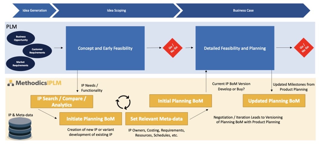
The Methodics recommended methodology is to start with a planning Bill of Material (BoM) to evaluate tradeoffs and perform analysis. Using a general-purpose Product Lifecycle Management (PLM) tool for 3rd party semiconductor components, and a semiconductor planning BoM tool for the in-house chip design, enables you to compare each approach. The combination of PLM and Methodics IP Lifecycle Management (IPLM) tools is shown below, as part of the build or buy decision process to improve your supply chain.

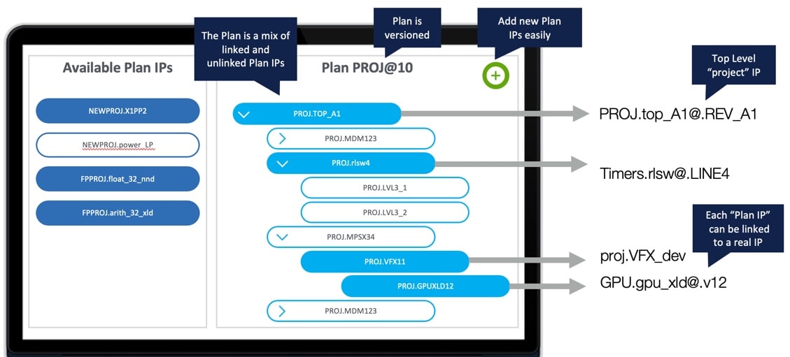
The Planning BoM has all of the details for each hierarchical IP being used, along with version history as each IP goes through a release cycle. Your team transitions from using the Planning BoM to an execution BoM while using the Perforce IPLM.

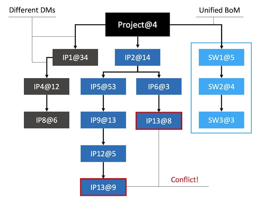
The IP hierarchy is defined in the Execution BoM and it should support popular data management tools like Git or Perforce Helix Core. Any version conflicts need to be automatically identified in both hardware and software IPs to keep compatibility.

Both hardware and software IPs are managed in this approach, making sure that requirements can be traced for every component. You will know which software component is delivered for each hardware component, ensuring transparency.
Release engineers are tasked with tracking each release candidate and managing the integration process, and using Methodics IPLM automates the manual integration and curation processes.
Meta-data can be used during the design process to account for ISO 26262 functional safety compliance requirements per IP. Traceability of requirements to IP blocks is captured with Methodics IPLM. Even security meta-data can be added on the IP or component hierarchy to help asses the security threats for each project, as you reference an internal IP Security Assurance (IPSA) catalog of issues for a circuit.
Summary
Systems companies are gradually adopting in-house IC design projects as a means to reduce supply chain bottlenecks. Using an IP-centric methodology is a best practice to control your ROI and start building IP re-use. The Methodics IPLM platform has been around for many years, helping to manage the challenges of IP-based design across entire corporations.
Benefits of this approach are: traceability of requirements, managing IP re-use, having a centralized catalog of all IP – hardware and software, having both planning and platform BoMs, and having analytics to see where you are at.
Read the entire nine page White Paper online here from Methodics.
Related Blogs
- The CHIPS and Science Act, Cybersecurity, and Semiconductor Manufacturing
- Solve Embedded Development Challenges With IP-Centric Planning
- WEBINAR: How to Improve IP Quality for Compliance
- Future of Semiconductor Design: 2022 Predictions and Trends
- Webinar – SoC Planning for a Modern, Component-Based Approach
- You Get What You Measure – How to Design Impossible SoCs with Perforce
- Achieving Scalability Means No More Silos


Comments
There are no comments yet.
You must register or log in to view/post comments.