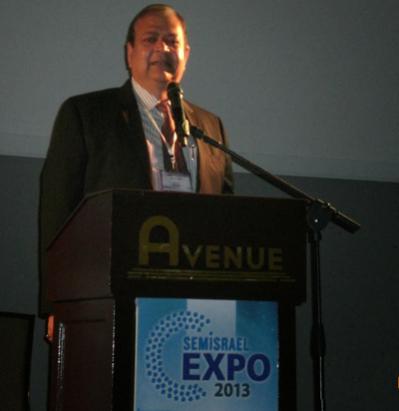
 Today at the Semisrael Expo 2013 (in Israel of course) Ajoy Bose gave a keynote on how design methodology will impact electronics. The big pictures is that microelectronics is driven by some major disruptive forces and, as a result, technology and industry are evolving dramatically, which creates a need for research and innovation and also new business opportunities.
What are these disruptive forces?
- Business: industry is now being driven by consumer and mobile
- Design: designing from scratch is being replaced by assembling blocks
- Technology: smaller technology nodes are creating new challenges for power, timing, test, routing congestion and more
- The conventional methods are being fractured
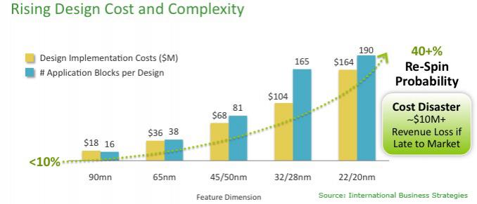
Of course the cost and complexity of designs has been rising fast in recent years. At 45nm an SoC design cost was about $68M and the SoC would contain about 81 blocks. By 22/20nm the cost has risen to $164M and the block count to 190. The probability of a re-spin is about 40% and, of course, is a disaster in terms of time-to-market.

And most of these are consumer markets: if your phone is not available in time for Christmas, you don’t get to sell it next March for less money since everyone will have bought a different phone. The speed of adoption of smartphones compared to older technologies such as television is astounding.
The methodologies to support block assembly type designs are not fully in place. One key is to move as much of design methodology up to the RTL level. It is possible to do a lot with signoff confidence at this level: test, power, congestion, clocks. The advantage of working at this level is that issues are discovered and fixed close to the source. Complexity is a lot reduced (a little RTL can generate a lot of gates and layout). And it is easier to do design exploration at this level. Of course, signoff still needs to be done after layout when all the details are in place. The purpose of the RTL-based approach is to ensure that very few problems remain to be dealt with.
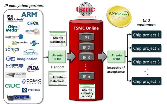
High quality IPs are the starting foundation for an SoC. By using tools such as Atrenta’s IP Kit which is based on SpyGlass then problems in the IP can be detected and fixed early, resulting in SpyGlass Clean IP. The big guys such as TSMC are using this approach. They make most of their money when chips go into volume production. So they have a strong incentive to reduce the delay from availability of IP and processes until production.
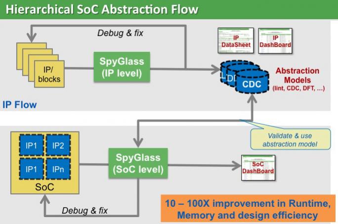
The volume of data is overwhelming. An approach based on hierarchical abstraction models is needed, retaining just enough of the internals to be able to assemble models and verify them against each other. This requires two sets of tools: at the IP level to create the models and at the SoC level to put them together and debug and fix any issues. With this approach run times and memory requirements can be reduced by 10x to 100x.
In the new mobile driven world, fast accurate SoC design is the key factor for success.
More articles by Paul McLellan…


Musk’s Orbital Compute Vision: TERAFAB and the End of the Terrestrial Data Center