In Part 1 of this topic I discussed what it takes to estimate the mean time between failures (MTBF) of a single stage synchronizer. Because supply voltages are decreasing and transistor thresholds have been pushed up to minimize leakage, the shortened MTBF of many synchronizer circuits at nanoscale process nodes is presenting an increased risk of failure. Moreover, new SoC designs are expected to have hundreds of clock domains and at least as many Clock Domain Crossings (CDCs). To decrease this risk of failure in these multi-synchronous designs, many designers routinely use multistage synchronizers in each CDC.
The following figure shows a typical multistage synchronizer. The N synchronizer stages are all clocked from the right-hand clock (fc), but data transitions produced in the left-hand clock domain (fd) may violate the setup and hold constraints of the first synchronizer flip-flop. These violations can result in metastable behavior of each of the N stages, but each added flip-flop reduces the width of the synchronizer’s window of vulnerability. Data transitions within that narrow window can cause serious mischief in the right-hand domain since the outputs from logic blocks L1 and L2 can then be inconsistent and lead to an unknown state. N must be chosen so that the chance of a data transition falling within the narrow window of vulnerability is extremely rare and the resulting MTBF is exceedingly long.

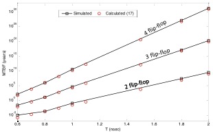
Today, two-stage (N=2) synchronizers are routine and three and four stages are becoming more common. However, the calculation of MTBF for these multistage devices is not straightforward. In fact, our recent paper, “MTBF bounds for multistage synchronizers” makes it clear that published MTBF models give widely varying results: the MTBF calculated at a single process corner and at a single operating condition gave results that varied over five orders of magnitude among the existing models. When compared with complete circuit simulation, our model gave consistently accurate results as shown in the following figure.

As one can see, calculated results can accurately predict simulated MTBF values. Some noteworthy comments about this result:
[LIST=1]
For the above figure, it is clear that at a 1 GHz clock rate, a 200 MHz data transition rate and the SS corner, this 90 nm single-stage, master-slave circuit was clearly unreliable for synchronizer service. A two-stage circuit has an MTBF of less than a year and even a three-stage circuit had an MTBF of less than 1000 years (considering you may have hundreds or even thousands of them in an ASIC, that’s still unreliable).
Risk of failure increases substantially at 45 nm and below, at lower supply voltages and at lower operating temperatures. Clearly, multistage synchronizers will find increasing use, particularly in multi-synchronous, custom silicon that goes into mission critical applications. Such applications include, for example, automotive engine control modules, lithium battery charger circuits, implantable medical devices, certain avionics products and industrial control systems. These designs should all have a critical sign-off covering all CDC MTBF specifications. The fact that it is not happening today is troubling.
lang: en_US
Share this post via:


Musk’s Orbital Compute Vision: TERAFAB and the End of the Terrestrial Data Center