There’s a nice article on timing closure by Dr. Jason Xing, Vice President of Engineering at ICScape Inc. on the Chip Design website. Not familiar with ICScape? Paul McLellan called ICScape the The Biggest EDA Company You’ve Never Heard Ofand Daniel Payne did Schematic, IC Layout, Clock and Timing Closure from ICScape at DAC, just to get you started.
Current IC designs have advanced quickly from 65 and 45 nanometers, down to 28, 20, and below. This progression to ever-smaller geometries has brought significant challenges in achieving timing closure to meet production deadlines and market windows. Engineering teams often struggle to efficiently perform late-stage ECOs (engineering change order) to meet their design as well as time to market objectives.
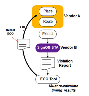
In the current methodology, engineers are forced to fix ECOs using two or more different tools in the flow, iterating far too many times, often just to meet production deadlines and market windows. This method of handling ECOs will get worse with each new process node. This brings up a dire need for a solution that will allow efficient and effective handling of ECOs and hence design closure.
What are the challenges with timing closure?
Jason Xing is co-founder and Vice President of Engineering at ICScape, where he architected clock and timing closure products. Jason has over 15 years EDA research and development experience. In 1997, He joined Sun Labs after receiving his PhD in Computer Science from the University of Illinois at Urbana-Champaign. At Sun Labs, Xing did research on physical and logical concurrent design methodologies and shape-based routing technologies. In 2001, he joined the Sun Microsystems internal CAD development team before he started ICScape in 2005. Jason holds another PhD in Mathematics from University of Louisiana.
ICScape is a leader in developing and delivering fast and accurate design closure solutions for today’s complex SOC designs, and a complete suite of analog and mixed-signal design, implementation and verification solutions. ICScape’s tools have been successfully used to design and deliver integrated circuits for a variety of application areas including storage, wireless, base band, data communications, multimedia, graphics, chipset and power management design. The solutions are silicon-proven through well over 100 tape-outs. The SOC design closure solutions fit into existing flows complementing signoff static timing analysis and physical design tools. While the analog / mixed-signal tools (AMS) form a complete solution, individual tools fit into existing AMS tool flows, preserving your current investment in tools.
ICScape now has a landing page on SemiWiki so you will be reading more about them soon. With all the EDA consolidation ICScape is the one to watch for both digital and analog solutions.


Musk’s Orbital Compute Vision: TERAFAB and the End of the Terrestrial Data Center