Multi-die system design is clearly gaining momentum. Part of this momentum focuses on chiplets and a chiplet ecosystem. A “building block” approach for design will work better if there is a way to get verified, quality building blocks in the form of chiplets. The recent Chiplet Summit became an epicenter for this topic. The conference grew about 2X from last year’s event. Chiplets are a hot topic. IO and memory chiplets are foundational elements for any system and a presentation on this topic by two companies making significant investments in this area caught my eye. Read on to see how Synopsys and Alchip accelerate IO & memory chiplet design for multi-die systems.
Who Presented

Presenting from Alchip was Erez Shaizaf, the company’s Chief Technology Officer. He is an industry veteran who focuses on system technology solutions based on 25-years of experience in VLSI, hardware, and system engineering. He has performed numerous successful silicon reticle tapeouts on advanced technology nodes and high-speed interfaces.

Presenting for Synopsys was Manmeet Walia, Product Director for Mixed-Signal PHY IP. I know Manmeet from my time at Synopsys. He has been managing mixed signal Interface IPs for HPC/Networking SoCs for over 14 years at Synopsys. Before that, he held marketing and system engineering leadership roles at AMCC, Exar, and Toshiba. Manmeet is quite knowledgeable and articulate.
This is a winning presentation team. Let’s see what topics were discussed.
About Multi-Die and Chiplets
There is a series of decisions to make regarding when it makes sense to move to multi-die design and what technology approach to take. The traditional approach of monolithic chip design will run into issues across a few areas. As the size of the die approaches the reticle limit, yield begins to suffer and the cost per die can become prohibitive. Now that multi-die integration strategies are becoming more available, splitting the design into multiple, smaller chips can be more cost-effective.
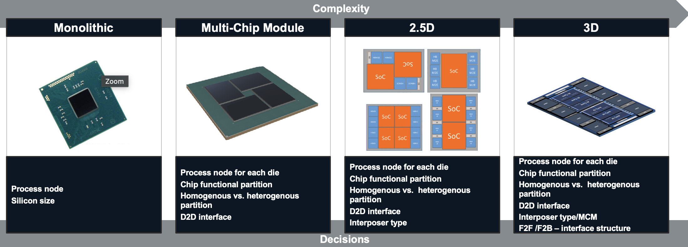
Beyond cost considerations are design flexibility and process optimization. The digital processing portion of a system may work best at the latest process node, but other parts of the system (memory or analog for example) will work best at different process nodes. Add to this the opportunity to acquire silicon-proven functions in chiplet form and design productivity and predictability can improve significantly. The figure below was presented to illustrate the continuum of choices.

The presenters outlined the decisions across performance and cost to create an ROI for the various approaches. Several designs across monolithic, 2.5D and 3D were then examined. It turns out there are quite a few choices to be made in each case and the ROI can vary quite a bit. This part of the presentation was eye-opening regarding the depth of decision-making required to examine all options.
Moving to either a 2.5 or 3D approach does have challenges. Some of those discussed include:
- Floor planning (TSV blockage)
- Clock delivery & timing signoff
- Power delivery
- Physical verification
- Thermal escape
In the area of chiplets, the following aspects were summarized:
Benefits
- Performance
- ROI
- Reusability
- TTM
Challenges
- Complex package
- NRE
- Die-to-die limited bandwidth
- Die-to-die power/latency
The conclusion was that there is no “one size fits all” solution. For each design, one must maximize the cost-performance ratio, which requires a custom-driven and not off-the-shelf approach. And there is a clear need for collaboration across EDA, IP, front-end, back-end, and package design.
Addressing the Design and IP Challenges
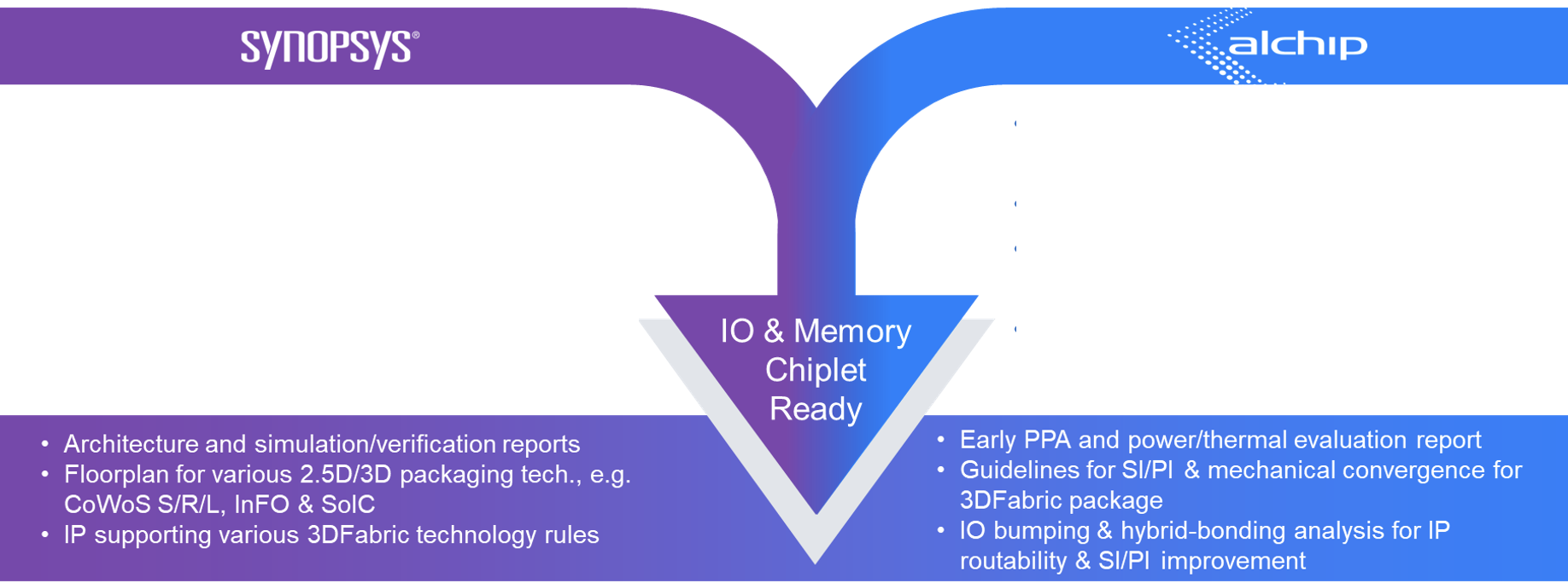
Both Alchip and Synopsys bring substantial capabilities to open a path to multi-die design. The approach for collaboration to help achieve multi-die system success from architecture partitioning, system design, IP integration, verification to high-volume manufacturing was explored in detail. The graphic at the top of this post is a good summary of how Synopsys and Alchip accelerate IO & memory chiplet design for multi-die systems. Here are some more relevant details for each company:

Regarding IO and memory chiplets, the value proposition was summarized this way:
Soft chiplet concept
- Reference design completed ahead of customer inquiry
- I/O and memory chiplets
- RTL data base including verification suite as subsystem
- Software drivers
- Debug tools
- Hardened for specified process node and package upon request
- Configurations, die size and aspect ratio changeable
Value proposition
- Splits monolithic SoC into chiplets
- Across multiple process nodes
- Across various packaging options
- Fast time-to-market
- Customers concentrate on core ASIC development
- Synopsys tier 1 IP with proven Alchip implementation
- Low risk – proven design and implementation
Alchip presented a new design platform called Chiptopia. The figure below summarizes the components of the platform.

The framework is summarized this way:
- Alchip, along with its customers, utilize the platform to collaboratively share design databases and workflows
- Enterprise and cloud-based installation
- RTL-to-GDS design automation
- Supports 2D, 2.5D and 3D design flow
- Use cases
- Augmented COT
- Resources augmentation
The main features include:
- Process node selection
- Application dependent
- Design library comparison
- P/G topology setups
- Clock strategy testing
And the key value statements include:
- Improved TTM
- Risk & cost reduction
The conclusion of the talk touched on the fact that one size does not fit all for package type, aspect ratio, and functionality. The focus needs to be on maximizing the cost-performance ratio. And this requires a custom-driven approach, NOT and off the shelf strategy. The collaboration between Alchip and Synopsys was described in detail, including EDA, IP, front-end, back-end, and package design.
A soft chiplet platform was described that supports hardening per customer application and selected package with shortened time-to-market, development, and volume.
SoC chiplets and the package go together with this strategy. And that’s how Synopsys and Alchip accelerate IO & memory chiplet design for multi-die systems.
Share this post via:


Comments
There are no comments yet.
You must register or log in to view/post comments.