You are currently viewing SemiWiki as a guest which gives you limited access to the site. To view blog comments and experience other SemiWiki features you must be a registered member. Registration is fast, simple, and absolutely free so please,
join our community today!
WP_Term Object
(
    [term_id] => 14433
    [name] => X-Subscriber
    [slug] => x-subscriber
    [term_group] => 0
    [term_taxonomy_id] => 14433
    [taxonomy] => category
    [description] =>
    [parent] => 0
    [count] => 0
    [filter] => raw
    [cat_ID] => 14433
    [category_count] => 0
    [category_description] =>
    [cat_name] => X-Subscriber
    [category_nicename] => x-subscriber
    [category_parent] => 0
    [is_post] =>
)
In this previous article, I was suggesting that certain chip makers may take a serious look at a disruptive way to look at Moore’s law, as they may get better ROI, profit and even better revenue. The idea is to select technology node and packaging technique in order to optimize the Price, Performance, Power triptych and manage chip… Read More
Moore’s Law has transcended computing expectations; however, its promise will eventually reach scalability limitations due to extraordinary consumer demands. Future technology encompasses breakthroughs capable of interaction with the outside world, which the More than Moore movement achieves. Through integrating … Read More
Tanner EDA is a pleasure to work with, they are big on collaboration and customers absolutely love their tools. With the Synopsys acquisition of SpringSoft, Tanner needs to step up and fill the void of the affordable Laker tools. Take a close look at their new v16 release and let me know how they are doing.
New capabilities for back-end… Read More
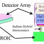
Image sensors are all around us with the cell phone being a popular example, and 35mm DSLR camera being another one. Last week I spoke with Kenton Veeder, an engineer at Senseeker that started his own image sensor IP and consulting services company. Instead of focusing on the consumer market, Kenton’s company does sensor … Read More
Back in 2011, TSMC announced it was extending its IP Alliance Program to include soft, or synthesizable IP. Around that time it was also announced that Atrenta’s SpyGlass platform would be used as the sole analysis tool to verify the completeness and quality of soft IP before being admitted to the program. Since then, the … Read More
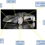
Embedded NVM technology based functions can be implemented in large SoC designed in advanced technology nodes down to 28nm, as there is no requirement for extra mask levels, like when integrating Nand Flash, negatively impacting the final cost. And it is also possible to integrate One Time Programmable (OTP) to store trim and … Read More
The most exciting EDA + Semi IP company that I ever worked at was Silicon Compilers in the 1980’s because it allowed you to start with a concept then implement to physical layout using a library of parameterized IP, the big problem was verifying that all of the IP combinations were in fact correct. Speed forward to today and our… Read More
While founder John Tanner, PhD, got his initial exposure to the TTL Cookbook and CMOS Cookbook as an undergraduate, it was his experience as a Caltech graduate student that forged his early path in EDA. In 1979, while enrolled in a VLSI design course at Caltech, John and his classmates received a pre-print of Carver Mead’s seminal… Read More
Sidense Corp. is a leading developer of embedded non-volatile memory (NVM) intellectual property (IP) for the semiconductor IC market. The company is headquartered in Ottawa, Canada, and has a global presence with sales offices worldwide.
The company was founded in 2004 by CTO Wlodek Kurjanowicz, a MoSys fellow and co-founder… Read More
Over at the GSA Forum website I have an article on the history of the semiconductor industry. It is actually based on a couple of brief history of semiconductor blogs (here and here) I published here on SemiWiki last year but edited down a lot and tightened up.
Since the start of the year seems to be the time for predictions, here are the… Read More