You are currently viewing SemiWiki as a guest which gives you limited access to the site. To view blog comments and experience other SemiWiki features you must be a registered member. Registration is fast, simple, and absolutely free so please,
join our community today!
WP_Term Object
(
    [term_id] => 14433
    [name] => X-Subscriber
    [slug] => x-subscriber
    [term_group] => 0
    [term_taxonomy_id] => 14433
    [taxonomy] => category
    [description] =>
    [parent] => 0
    [count] => 0
    [filter] => raw
    [cat_ID] => 14433
    [category_count] => 0
    [category_description] =>
    [cat_name] => X-Subscriber
    [category_nicename] => x-subscriber
    [category_parent] => 0
    [is_post] =>
)
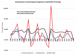
Because of significant $4 billion in equipment pull-ins in Q4 from sales in Asia, I was reducing my semiconductor wafer front-end (WFE) equipment revenue growth from an earlier +5% to 0% in 2020. Now, based on CORVID-19, I am further reducing revenue growth to -6.9%.
Chart 1 also shows the cyclical nature of semiconductors and semiconductor… Read More
It is predicted that by 2030 energy consumption attributable to data centers will make up a staggering 8% of the world’s total usage!
As we move in to 2020 it’s clear that every sector of industry, including the semiconductor industry, will have a responsibility to address growing environmental concerns. We should be aware that… Read More
If it’s your job to get a SoC design through synthesis, timing/power closure and final verification, the last thing you need are surprises in new versions of the IP blocks that are integrated into the design. If your IP supplier sends a new version, the best possible scenario is that this is only a small incremental change from… Read More
The rate of product development is facing very real challenges as the pace of silicon technology evolution begins to slow. Today, we are squeezing the most out of transistor physics, which is essentially derived from 60-year-old CMOS technology. To maintain the pace of Moore’s law, it is predicted that in 2030 we will need transistors… Read More
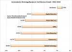
KLA saw its share of the semiconductor metrology/inspection market increase from 52% in 2018 to 56% in 2019.
As a background, KLA manufactures and sells equipment used to monitor many of the 400 to 600 processing steps in the manufacturing of semiconductors, starting with a bare wafer, such as silicon, to a completed device. The… Read More
The Future Of Embedded Monitoring – February 2020by Stephen Crosher on 02-14-2020 at 10:00 amCategories: IP, Moortec
Shall I compare thee to a…Rolls Royce jet engine?
‘There is a new era dawning whereby deeply embedded sensing within all technology will bring about great benefit for the reliability and performance of semiconductor-based products.’ These were my words during a presentation to an industry audience in China back in September… Read More
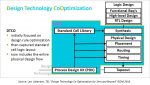
SLiC Library tool dramatically accelerates DTCO for 3nm and beyond
In advanced technology nodes below 10nm, Design and Process Technology development have become increasingly intertwined. In older nodes the traditional technology roll-out was done mostly in a sequential manner with clear geometry scaling targets set by … Read More
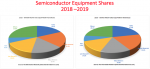
For the first time since 1990, Applied Materials is poised to lose its lead in the semiconductor equipment market, according to my recently published report “The Global Semiconductor Equipment: Markets, Market Shares, Market Forecasts.”
Applied Materials, which has been losing market share in the wafer front end (WFE) equipment… Read More
One of the reasons I founded SemiWiki nine years ago was the lack of EDA, IP and Foundry content in the media. The problem is that unless you work in the industry it is very difficult to write about it in competent technical detail. Most media outlets only know what vendors tell them which is how the semiconductor industry worked before… Read More
Lam Research (NASDAQ:LRCX) will announce its quarterly earnings on October 23, 2019, and Applied Materials (NASDAQ:AMAT) the following month on November 14, 2019. Both companies make equipment used to manufacture semiconductor devices. While private and institutional investors often own both individual stocks, this article… Read More