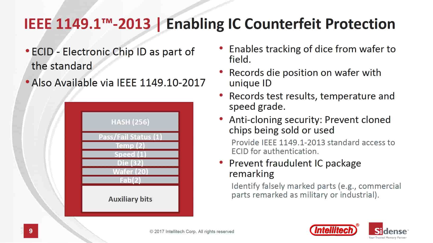
As chips for any design are fabricated, it turns out that no two are the exactly the same. This is both a blessing and a curse. Current silicon fabrication technology is amazingly good at controlling factors that affect chip to chip uniformity. Nevertheless, each chip has different characteristics. The most extreme case of happens… Read More
AI Based Software Designing AI Based Hardware – Autonomous Automotive SoC Platform
For those of you who missed the NetSpeed Systems, Imagination Technologies webinar, “Alexa, can you help me build a better SoC”, you’ll be happy to hear that the session was recorded and can still be viewed (see link at the bottom of this page). I’ll warn you now however, that this was a high-bandwidth session packed with information,… Read More
Enabling a New Semiconductor Revolution!
According to semiconductor trade statistics, 2017 will be the strongest market since 2010 easily recording double digit gains causing the SOX Semiconductor Index to outpace NASDAQ and the other indexes. The question Wall Street people have now is: How much longer will semiconductors be an attractive investment? That question… Read More
Presto Engineering – Outsourced Secure Provisioning – Even Their Secrets Have Secrets
When I first heard about Presto Engineering I was enamored by a statement on their web site that claimed that one of their secured solutions included, “The ability to incorporate your secrets without knowing them”. If Mr. Spock would have been in the room his eyebrow would have certainly raised. Indeed, what does that statement … Read More
Adoption, Architecture and Origami
Last week I sat in on Oski’s latest in a series of “Decoding Formal” sessions. Judging by my first experience, they plan and manage these events very well. Not too long (~3 hours of talks), good food (DishDash), good customer content, a good forward-looking topic and a very entertaining wrap-up talk.… Read More
Robust NVM Solutions for Specialty and Advanced FinFET Technologies Webinar
Webinars are a very effective communications channel in a fast paced industry like semiconductor design. If you sign-up in advance and you can’t make the live version, you will be automatically notified when the replay is available so you can watch it at your leisure. I’m guilty of this for sure, because of my hectic… Read More
Intrinsix Fields Ultra-Low Power Security IP for the IoT Market
As the Internet-of-Things (IoT) market continues to grow, the industry is coming to grips with the need to secure their IoT systems across the entire spectrum of IoT devices (edge, gateway, and cloud). One need only look back to the 2016 distributed denial-of-service (DDoS) attacks that caused internet outages for major portions… Read More
Yield Analysis is a Critical Driver for Profitability
One of the most important aspects of any manufacturing effort is the yield of the process. Today, the investment in facilities, equipment and materials is so high that consistently high yields are vital to the profitability of the semiconductor manufacturer. Furthermore, the engineers must get to that consistent high yield … Read More
Semiconductor Device Physics, Lab in a Box
One of my favorite classes in college was the lab exercise, mostly because we actually got to use real electronics and then measure something, finally writing it up in our lab notebooks. The issue today is that a college student taking Electrical Engineering probably doesn’t have much access to 10nm FinFET silicon for use… Read More
Webinar Preview: Alexa, can you help me build a better SoC?
Nothing is pushing complexity in system-on-chips (SoCs) designs like the drive (no pun intended) to make autonomous vehicles a widespread reality. Autonomous vehicle systems require heterogeneous architectures with reliable, efficient communications between CPU clusters, vision processing accelerators, storage and… Read More


