You are currently viewing SemiWiki as a guest which gives you limited access to the site. To view blog comments and experience other SemiWiki features you must be a registered member. Registration is fast, simple, and absolutely free so please,
join our community today!
            WP_Term Object
(
    [term_id] => 24
    [name] => TSMC
    [slug] => tsmc
    [term_group] => 0
    [term_taxonomy_id] => 24
    [taxonomy] => category
    [description] =>
    [parent] => 158
    [count] => 621
    [filter] => raw
    [cat_ID] => 24
    [category_count] => 621
    [category_description] =>
    [cat_name] => TSMC
    [category_nicename] => tsmc
    [category_parent] => 158
    [is_post] =>
)

WP_Term Object
(
    [term_id] => 24
    [name] => TSMC
    [slug] => tsmc
    [term_group] => 0
    [term_taxonomy_id] => 24
    [taxonomy] => category
    [description] =>
    [parent] => 158
    [count] => 621
    [filter] => raw
    [cat_ID] => 24
    [category_count] => 621
    [category_description] =>
    [cat_name] => TSMC
    [category_nicename] => tsmc
    [category_parent] => 158
    [is_post] =>
)
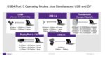
When USB initially came out it revolutionized how peripherals connect to host systems. We all remember when Apple did away with many separate connections for mouse, keyboard, audio and more with their first computers supporting USB. USB has continued to develop more flexibility and more throughput. In 2015 Apple again introduced… Read More
Recently, TSMC held their 26th annual Technology Symposium, which was conducted virtually for the first time. This article is the last of three that attempts to summarize the highlights of the presentations. This article focuses on the technology design enablement roadmap, as described by Cliff Hou, SVP, R&D.
Key Takeaways… Read More
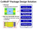
Recently, TSMC held their 26th annual Technology Symposium, which was conducted virtually for the first time. This article is the second of three that attempts to summarize the highlights of the presentations. This article focuses on the TSMC advanced packaging technology roadmap, as described by Doug Yu, VP, R&D.
Key… Read More
Recently, TSMC held their 26th annual Technology Symposium, which was conducted virtually for the first time. This article is the first of three that attempts to summarize the highlights of the presentations.
This article focuses on the TSMC process technology roadmap, as described by the following executives:
…
Read More
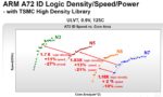
This comparison of smartphone processors from different companies and fab processes was originally going to be a post, but with the growing information content, I had to put it into an article. Here, due to information availability, Apple, Huawei, and Samsung Exynos processors will get the most coverage, but a few Qualcomm Snapdragon
…
Read More
Summary
Thermo-compression bonding is used in heterogeneous 3D packaging technology – this attach method was applied to the assembly of large (12-stack and 16-stack) high bandwidth memory (HBM) die, with significant bandwidth and power improvements over traditional microbump attach.
Introduction
The rapid growth of heterogeneous… Read More
Waving white surrender flag as TSMC dominates-
The quarter was a success but the patient is dying-
Packaging now critical as Moore progress stumbles-
Intel reported a great quarter but weak H2 guidance-
But 7NM slip and “fab lite” talk sends shockwaves-
Intel reported a great quarter beating numbers all around with… Read More
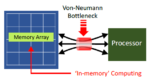
“AI is the new electricity.”, according to Andrew Ng, Professor at Stanford University. The potential applications for machine learning classification are vast. Yet, current ML inference techniques are limited by the high power dissipation associated with traditional architectures. The figure below highlights the … Read More
There have been a multitude of announcements recently relative to the incorporation of machine learning (ML) methods into EDA tool algorithms, mostly in the physical implementation flows. For example, deterministic ML-based decision algorithms applied to cell placement and signal interconnect routing promise to expedite… Read More
Summary
The growing significance of ultra-short reach (USR) interfaces on 2.5D packaging technology has led to a variety of electrical definitions and circuit implementations. TSMC recently presented the approach adopted by their IP development team, for a parallel-bus, clock-forwarded USR interface to optimize power/performance/area… Read More