You are currently viewing SemiWiki as a guest which gives you limited access to the site. To view blog comments and experience other SemiWiki features you must be a registered member. Registration is fast, simple, and absolutely free so please,
join our community today!
WP_Term Object
(
    [term_id] => 50
    [name] => Events
    [slug] => events
    [term_group] => 0
    [term_taxonomy_id] => 50
    [taxonomy] => category
    [description] =>
    [parent] => 0
    [count] => 1522
    [filter] => raw
    [cat_ID] => 50
    [category_count] => 1522
    [category_description] =>
    [cat_name] => Events
    [category_nicename] => events
    [category_parent] => 0
    [is_post] =>
)
On my flight to Las Vegas for the annual Consumer Electronics show I dug in to Jeff Smulyan’s autobiographical “Never Ride a RollerCoaster Upside Down – The Ups and Downs and Reinvention of an Entrepreneur.” As CEO, Chairman, and Founder of Emmis Communications Smulyan has had a front row seat to the evolution of the electronics… Read More
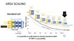
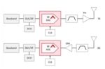
At the IEDM conference in December 2022, Imec presented “Semi-damascene Integration of a 2-layer MOL VHV Scaling Booster to Enable 4-track Standard Cells,” I had a chance to not only read the paper and see it presented, but also to interview one of the authors Zsolt Tokie.
Logic designs are built up by standard cells such as inverters,… Read More
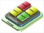
The first Chiplet specific conference is coming up which is a milestone in itself. As we know the only thing new about chiplets is the name but when there is a dedicated conference to such a specific thing you know it has officially “arrived”. There is even a cool new tagline: Chiplets make huge chips happen!
“The First Annual Chiplet… Read More
CES 2023, the annual consumer technology show, was held last week in Las Vegas, Nevada. Over 115,000 people attended and over 3200 companies exhibited. As shown below, attendance and exhibitors were up about 2 ½ times the pandemic limited CES 2022. However, attendance was down one-third and exhibitors were down 27% from CES 2020.… Read More
It’s January so time for me to review what I’ve found at CES this year that relates to cycling. Unlike last year when there were many last-minute cancellations from exhibitors, in 2023 it’s in-person and bigger than ever. The electrification of bikes continues, and many of these electronic devices are cloud… Read More
One of the first events on the 2023 EDA calendar is the Phil Kaufman Award ceremony and banquet honoring the 2022 recipient Dr. Giovanni De Micheli. The event, hosted by the Electronic System Design Alliance (ESD Alliance) and the IEEE Council on Electronic Design Automation (CEDA), will be held Thursday, February 23, starting… Read More
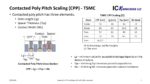
TSMC presented two papers on 3nm at the 2022 IEDM; “Critical Process features Enabling Aggressive Contacted Gate Pitch Scaling for 3nm CMOS Technology and Beyond” and “A 3nm CMOS FinFlexTM Platform Technology with Enhanced Power Efficiency and Performance for Mobile SOC and High Performance Computing Applications”.
When … Read More
Sensors are inherently analog in nature, and they get digitized for processing by using an Analog to Digital Converter (ADC) block. At the recent IP SoC event I had the chance to see the presentation by Ken Potts, COO of Alphacore on their semiconductor IP for ADCs. I learned that Alphacore started out in 2012, now offering both standard… Read More
Building next generation systems is a real balancing act. The high-performance computing demands presented by increasing AI an ML content in systems means there are increasing challenges for power consumption, thermal load, and the never-ending appetite for faster data communications. Power, performance, and cooling … Read More
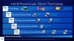
Ann Kelleher is Intel’s Executive Vice President, General Manager, Technology Development, and she gave the first plenary talk to kick off the 2022 IEDM, “Celebrating 75 Years of the Transistor A Look at the Evolution of Moore’s Law Innovation”. I am generally not a fan of plenary talks because I think they are often too broad and… Read More


Agentic AI Demands More Than GPUs