Through my contacts at SemiWiki I was introduced to a mixed signal IP company named SilabTech, and then decided to interview the founder and CEO, Sujoy Chakravarty.
Sujoy Chakravarty, CEO and Founder
… Read More
            WP_Term Object
(
    [term_id] => 159
    [name] => Siemens EDA
    [slug] => siemens-eda
    [term_group] => 0
    [term_taxonomy_id] => 159
    [taxonomy] => category
    [description] =>
    [parent] => 157
    [count] => 841
    [filter] => raw
    [cat_ID] => 159
    [category_count] => 841
    [category_description] =>
    [cat_name] => Siemens EDA
    [category_nicename] => siemens-eda
    [category_parent] => 157
    [is_post] =>
)

WP_Term Object
(
    [term_id] => 159
    [name] => Siemens EDA
    [slug] => siemens-eda
    [term_group] => 0
    [term_taxonomy_id] => 159
    [taxonomy] => category
    [description] =>
    [parent] => 157
    [count] => 841
    [filter] => raw
    [cat_ID] => 159
    [category_count] => 841
    [category_description] =>
    [cat_name] => Siemens EDA
    [category_nicename] => siemens-eda
    [category_parent] => 157
    [is_post] =>
)

Through my contacts at SemiWiki I was introduced to a mixed signal IP company named SilabTech, and then decided to interview the founder and CEO, Sujoy Chakravarty.
Sujoy Chakravarty, CEO and Founder
… Read More
The growing amount of electronics within today’s automobiles is driving very high quality and reliability requirements to a widening range of semiconductor devices. At the same time, traditional fault models are becoming less effective at achieving desired silicon quality levels. Improvements in test solutions are needed… Read More
On the Tuesday of DAC I moderated a panel session on Hardware Assisted Verification in 10 Years: More Need, More Speed. Although this topic obviously could include FPGA-based prototyping, in fact we spent pretty much the whole time talking about emulation. Gary Smith, on Sunday night, actually set up things by pointing out that… Read More
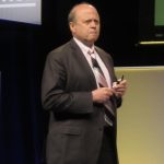
One new feature at DAC this year is that several of the keynotes are preceded by a ten minute vision of the future from one of the EDA CEOs. Today it was Wally Rhines’s turn. Wally is CEO of Mentor Graphics. He titled his talk Changing the World Through EDA. Since EDA as we know it started in the late 1970s, the number of transistors… Read More

Robust Reliability Verification: Beyond Traditional Tools
by Matthew Hogan, Mentor Graphics
At all process nodes, countless hours are diligently expended to ensure that our integrated circuit (IC) designs will function in the way we intended, can be manufactured with satisfactory yields, and are delivered in a timely fashion… Read More
What: DAC lunch seminar (register here)
When: June 5, 2013, 11:30am – 1:30pm
Where: At DAC in lovely Austin, TX
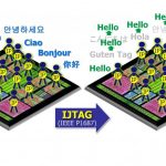
Dr. Martin Keim of Mentor Graphics will present this overview of the new the IEEE P1687 standard, called IJTAG for ‘internal’ JTAG.
If you are involved in IC test*, you’ve probably heard about IJTAG. If you … Read More
DAC 2013 is closing in fast now…and if you haven’t made your plans for what you want to see and do, you’d better get going! Of course, I’m happy to help you out with a few suggestions…starting with that most important objective—conference swag. Stop by the Mentor Graphics booth (#2046, for those of you who actually look at your floor… Read More

One of the most useful ways to learn about an EDA tool is to talk with other users that have experience with that tool. IC Place and Route tools are complex and yet necessary to implement every SoC designed today, so at DAC in just two weeks you have a chance to hear first-hand from several P&R tool users. To get a better idea about these… Read More
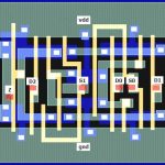
You may have heard about cell-aware testing. It’s a transistor-level test (ATPG) methodology that is quickly becoming a hot topic. If you are involved in DFT and are looking for better quality and reliability, you should definitely know about cell-aware testing.
And lucky you, on May 16, 2013, you can attend a free seminar on cell-aware… Read More
You will never meet a more approachable CEO in the semiconductor ecosystem than Dr. Walden C. Rhines. The first time I met Wally was way back when I blogged for food and he invited me over for lunch. Even better, a year or two later I was having dinner with a friend at the DBL Tree in San Jose. Wally was waiting for his flight home so he joined… Read More
Array
(
    [node_name] => Siemens EDA
    [node_id] => Array
        (
            [0] => 2
        )

)
XF\Mvc\Entity\ArrayCollection Object
(
    [entities:protected] => Array
        (
            [367] => XF\Entity\Node Object
                (
                    [_uniqueEntityId:XF\Mvc\Entity\Entity:private] => 54
                    [rootClass:protected] => XF\Entity\Node
                    [_useReplaceInto:protected] =>
                    [_newValues:protected] => Array
                        (
                        )

                    [_values:protected] => Array
                        (
                            [node_id] => 367
                            [title] => Siemens EDA
                            [description] =>
                            [node_name] =>
                            [node_type_id] => Forum
                            [parent_node_id] => 355
                            [display_order] => 380
                            [display_in_list] => 1
                            [lft] => 87
                            [rgt] => 88
                            [depth] => 2
                            [style_id] => 0
                            [effective_style_id] => 4
                            [breadcrumb_data] => {"385":{"node_id":385,"title":"Companies","depth":0,"lft":13,"node_name":null,"node_type_id":"LinkForum","display_in_list":true},"355":{"node_id":355,"title":"Company Forums","depth":1,"lft":14,"node_name":null,"node_type_id":"Category","display_in_list":true}}
                            [navigation_id] =>
                            [effective_navigation_id] =>
                        )

                    [_relations:protected] => Array
                        (
                        )

                    [_previousValues:protected] => Array
                        (
                        )

                    [_options:protected] => Array
                        (
                        )

                    [_deleted:protected] =>
                    [_readOnly:protected] =>
                    [_writePending:protected] =>
                    [_writeRunning:protected] =>
                    [_errors:protected] => Array
                        (
                        )

                    [_whenSaveable:protected] => Array
                        (
                        )

                    [_cascadeSave:protected] => Array
                        (
                        )

                    [_behaviors:protected] =>
                )

        )

    [populated:protected] => 1
)
XF\Mvc\Entity\ArrayCollection Object
(
[entities:protected] => Array
(
[25563] => ThemeHouse\XPress\XF\Entity\Thread Object
(
[_uniqueEntityId:XF\Mvc\Entity\Entity:private] => 55
[rootClass:protected] => XF\Entity\Thread
[_useReplaceInto:protected] =>
[_newValues:protected] => Array
(
)
[_values:protected] => Array
(
[thread_id] => 25563
[node_id] => 367
[title] => Siemens to acquire Precision Innovations to expand AI-powered system-on-a-chip design exploration and optimization
[reply_count] => 0
[view_count] => 38
[user_id] => 25277
[username] => AmandaK
[post_date] => 1784589643
[sticky] => 0
[discussion_state] => visible
[discussion_open] => 1
[discussion_type] => discussion
[first_post_id] => 101925
[first_post_reaction_score] => 0
[first_post_reactions] => []
[last_post_date] => 1784589643
[last_post_id] => 101925
[last_post_user_id] => 25277
[last_post_username] => AmandaK
[prefix_id] => 0
[tags] => []
[custom_fields] => []
[vote_score] => 0
[vote_count] => 0
[featured] => 0
[type_data] => []
[index_state] => default
)
[_relations:protected] => Array
(
[Forum] => XF\Entity\Forum Object
(
[_uniqueEntityId:XF\Mvc\Entity\Entity:private] => 76
[rootClass:protected] => XF\Entity\Forum
[_useReplaceInto:protected] =>
[_newValues:protected] => Array
(
)
[_values:protected] => Array
(
[node_id] => 367
[discussion_count] => 451
[message_count] => 455
[last_post_id] => 101925
[last_post_date] => 1784589643
[last_post_user_id] => 25277
[last_post_username] => AmandaK
[last_thread_id] => 25563
[last_thread_title] => Siemens to acquire Precision Innovations to expand AI-powered system-on-a-chip design exploration and optimization
[last_thread_prefix_id] => 0
[moderate_threads] => 1
[moderate_replies] => 1
[allow_posting] => 1
[count_messages] => 1
[auto_feature] => 0
[find_new] => 1
[allow_index] => allow
[index_criteria] =>
[field_cache] => []
[prefix_cache] => []
[prompt_cache] => []
[default_prefix_id] => 0
[default_sort_order] => last_post_date
[default_sort_direction] => desc
[list_date_limit_days] => 0
[require_prefix] => 0
[allowed_watch_notifications] => all
[min_tags] => 0
[forum_type_id] => discussion
[type_config] => {"allowed_thread_types":["poll"],"allow_answer_voting":false,"allow_answer_downvote":false}
)
[_relations:protected] => Array
(
[Node] => XF\Entity\Node Object
(
[_uniqueEntityId:XF\Mvc\Entity\Entity:private] => 54
[rootClass:protected] => XF\Entity\Node
[_useReplaceInto:protected] =>
[_newValues:protected] => Array
(
)
[_values:protected] => Array
(
[node_id] => 367
[title] => Siemens EDA
[description] =>
[node_name] =>
[node_type_id] => Forum
[parent_node_id] => 355
[display_order] => 380
[display_in_list] => 1
[lft] => 87
[rgt] => 88
[depth] => 2
[style_id] => 0
[effective_style_id] => 4
[breadcrumb_data] => {"385":{"node_id":385,"title":"Companies","depth":0,"lft":13,"node_name":null,"node_type_id":"LinkForum","display_in_list":true},"355":{"node_id":355,"title":"Company Forums","depth":1,"lft":14,"node_name":null,"node_type_id":"Category","display_in_list":true}}
[navigation_id] =>
[effective_navigation_id] =>
)
[_relations:protected] => Array
(
)
[_previousValues:protected] => Array
(
)
[_options:protected] => Array
(
)
[_deleted:protected] =>
[_readOnly:protected] =>
[_writePending:protected] =>
[_writeRunning:protected] =>
[_errors:protected] => Array
(
)
[_whenSaveable:protected] => Array
(
)
[_cascadeSave:protected] => Array
(
)
[_behaviors:protected] =>
)
)
[_previousValues:protected] => Array
(
)
[_options:protected] => Array
(
)
[_deleted:protected] =>
[_readOnly:protected] =>
[_writePending:protected] =>
[_writeRunning:protected] =>
[_errors:protected] => Array
(
)
[_whenSaveable:protected] => Array
(
)
[_cascadeSave:protected] => Array
(
)
[_behaviors:protected] =>
)
[25562] => ThemeHouse\XPress\XF\Entity\Thread Object
(
[_uniqueEntityId:XF\Mvc\Entity\Entity:private] => 56
[rootClass:protected] => XF\Entity\Thread
[_useReplaceInto:protected] =>
[_newValues:protected] => Array
(
)
[_values:protected] => Array
(
[thread_id] => 25562
[node_id] => 367
[title] => Survey Findings Point to Technology as the Key to Power Grid Resilience
[reply_count] => 0
[view_count] => 28
[user_id] => 25277
[username] => AmandaK
[post_date] => 1784589092
[sticky] => 0
[discussion_state] => visible
[discussion_open] => 1
[discussion_type] => discussion
[first_post_id] => 101924
[first_post_reaction_score] => 0
[first_post_reactions] => []
[last_post_date] => 1784589092
[last_post_id] => 101924
[last_post_user_id] => 25277
[last_post_username] => AmandaK
[prefix_id] => 0
[tags] => []
[custom_fields] => []
[vote_score] => 0
[vote_count] => 0
[featured] => 0
[type_data] => []
[index_state] => default
)
[_relations:protected] => Array
(
[Forum] => XF\Entity\Forum Object
(
[_uniqueEntityId:XF\Mvc\Entity\Entity:private] => 76
[rootClass:protected] => XF\Entity\Forum
[_useReplaceInto:protected] =>
[_newValues:protected] => Array
(
)
[_values:protected] => Array
(
[node_id] => 367
[discussion_count] => 451
[message_count] => 455
[last_post_id] => 101925
[last_post_date] => 1784589643
[last_post_user_id] => 25277
[last_post_username] => AmandaK
[last_thread_id] => 25563
[last_thread_title] => Siemens to acquire Precision Innovations to expand AI-powered system-on-a-chip design exploration and optimization
[last_thread_prefix_id] => 0
[moderate_threads] => 1
[moderate_replies] => 1
[allow_posting] => 1
[count_messages] => 1
[auto_feature] => 0
[find_new] => 1
[allow_index] => allow
[index_criteria] =>
[field_cache] => []
[prefix_cache] => []
[prompt_cache] => []
[default_prefix_id] => 0
[default_sort_order] => last_post_date
[default_sort_direction] => desc
[list_date_limit_days] => 0
[require_prefix] => 0
[allowed_watch_notifications] => all
[min_tags] => 0
[forum_type_id] => discussion
[type_config] => {"allowed_thread_types":["poll"],"allow_answer_voting":false,"allow_answer_downvote":false}
)
[_relations:protected] => Array
(
[Node] => XF\Entity\Node Object
(
[_uniqueEntityId:XF\Mvc\Entity\Entity:private] => 54
[rootClass:protected] => XF\Entity\Node
[_useReplaceInto:protected] =>
[_newValues:protected] => Array
(
)
[_values:protected] => Array
(
[node_id] => 367
[title] => Siemens EDA
[description] =>
[node_name] =>
[node_type_id] => Forum
[parent_node_id] => 355
[display_order] => 380
[display_in_list] => 1
[lft] => 87
[rgt] => 88
[depth] => 2
[style_id] => 0
[effective_style_id] => 4
[breadcrumb_data] => {"385":{"node_id":385,"title":"Companies","depth":0,"lft":13,"node_name":null,"node_type_id":"LinkForum","display_in_list":true},"355":{"node_id":355,"title":"Company Forums","depth":1,"lft":14,"node_name":null,"node_type_id":"Category","display_in_list":true}}
[navigation_id] =>
[effective_navigation_id] =>
)
[_relations:protected] => Array
(
)
[_previousValues:protected] => Array
(
)
[_options:protected] => Array
(
)
[_deleted:protected] =>
[_readOnly:protected] =>
[_writePending:protected] =>
[_writeRunning:protected] =>
[_errors:protected] => Array
(
)
[_whenSaveable:protected] => Array
(
)
[_cascadeSave:protected] => Array
(
)
[_behaviors:protected] =>
)
)
[_previousValues:protected] => Array
(
)
[_options:protected] => Array
(
)
[_deleted:protected] =>
[_readOnly:protected] =>
[_writePending:protected] =>
[_writeRunning:protected] =>
[_errors:protected] => Array
(
)
[_whenSaveable:protected] => Array
(
)
[_cascadeSave:protected] => Array
(
)
[_behaviors:protected] =>
)
)
[_previousValues:protected] => Array
(
)
[_options:protected] => Array
(
)
[_deleted:protected] =>
[_readOnly:protected] =>
[_writePending:protected] =>
[_writeRunning:protected] =>
[_errors:protected] => Array
(
)
[_whenSaveable:protected] => Array
(
)
[_cascadeSave:protected] => Array
(
)
[_behaviors:protected] =>
)
[25536] => ThemeHouse\XPress\XF\Entity\Thread Object
(
[_uniqueEntityId:XF\Mvc\Entity\Entity:private] => 57
[rootClass:protected] => XF\Entity\Thread
[_useReplaceInto:protected] =>
[_newValues:protected] => Array
(
)
[_values:protected] => Array
(
[thread_id] => 25536
[node_id] => 367
[title] => Siemens and Cloudberry VC collaborate to accelerate European deep-tech innovation
[reply_count] => 0
[view_count] => 200
[user_id] => 25277
[username] => AmandaK
[post_date] => 1784251672
[sticky] => 0
[discussion_state] => visible
[discussion_open] => 1
[discussion_type] => discussion
[first_post_id] => 101815
[first_post_reaction_score] => 0
[first_post_reactions] => []
[last_post_date] => 1784251672
[last_post_id] => 101815
[last_post_user_id] => 25277
[last_post_username] => AmandaK
[prefix_id] => 0
[tags] => []
[custom_fields] => []
[vote_score] => 0
[vote_count] => 0
[featured] => 0
[type_data] => []
[index_state] => default
)
[_relations:protected] => Array
(
[Forum] => XF\Entity\Forum Object
(
[_uniqueEntityId:XF\Mvc\Entity\Entity:private] => 76
[rootClass:protected] => XF\Entity\Forum
[_useReplaceInto:protected] =>
[_newValues:protected] => Array
(
)
[_values:protected] => Array
(
[node_id] => 367
[discussion_count] => 451
[message_count] => 455
[last_post_id] => 101925
[last_post_date] => 1784589643
[last_post_user_id] => 25277
[last_post_username] => AmandaK
[last_thread_id] => 25563
[last_thread_title] => Siemens to acquire Precision Innovations to expand AI-powered system-on-a-chip design exploration and optimization
[last_thread_prefix_id] => 0
[moderate_threads] => 1
[moderate_replies] => 1
[allow_posting] => 1
[count_messages] => 1
[auto_feature] => 0
[find_new] => 1
[allow_index] => allow
[index_criteria] =>
[field_cache] => []
[prefix_cache] => []
[prompt_cache] => []
[default_prefix_id] => 0
[default_sort_order] => last_post_date
[default_sort_direction] => desc
[list_date_limit_days] => 0
[require_prefix] => 0
[allowed_watch_notifications] => all
[min_tags] => 0
[forum_type_id] => discussion
[type_config] => {"allowed_thread_types":["poll"],"allow_answer_voting":false,"allow_answer_downvote":false}
)
[_relations:protected] => Array
(
[Node] => XF\Entity\Node Object
(
[_uniqueEntityId:XF\Mvc\Entity\Entity:private] => 54
[rootClass:protected] => XF\Entity\Node
[_useReplaceInto:protected] =>
[_newValues:protected] => Array
(
)
[_values:protected] => Array
(
[node_id] => 367
[title] => Siemens EDA
[description] =>
[node_name] =>
[node_type_id] => Forum
[parent_node_id] => 355
[display_order] => 380
[display_in_list] => 1
[lft] => 87
[rgt] => 88
[depth] => 2
[style_id] => 0
[effective_style_id] => 4
[breadcrumb_data] => {"385":{"node_id":385,"title":"Companies","depth":0,"lft":13,"node_name":null,"node_type_id":"LinkForum","display_in_list":true},"355":{"node_id":355,"title":"Company Forums","depth":1,"lft":14,"node_name":null,"node_type_id":"Category","display_in_list":true}}
[navigation_id] =>
[effective_navigation_id] =>
)
[_relations:protected] => Array
(
)
[_previousValues:protected] => Array
(
)
[_options:protected] => Array
(
)
[_deleted:protected] =>
[_readOnly:protected] =>
[_writePending:protected] =>
[_writeRunning:protected] =>
[_errors:protected] => Array
(
)
[_whenSaveable:protected] => Array
(
)
[_cascadeSave:protected] => Array
(
)
[_behaviors:protected] =>
)
)
[_previousValues:protected] => Array
(
)
[_options:protected] => Array
(
)
[_deleted:protected] =>
[_readOnly:protected] =>
[_writePending:protected] =>
[_writeRunning:protected] =>
[_errors:protected] => Array
(
)
[_whenSaveable:protected] => Array
(
)
[_cascadeSave:protected] => Array
(
)
[_behaviors:protected] =>
)
)
[_previousValues:protected] => Array
(
)
[_options:protected] => Array
(
)
[_deleted:protected] =>
[_readOnly:protected] =>
[_writePending:protected] =>
[_writeRunning:protected] =>
[_errors:protected] => Array
(
)
[_whenSaveable:protected] => Array
(
)
[_cascadeSave:protected] => Array
(
)
[_behaviors:protected] =>
)
[25535] => ThemeHouse\XPress\XF\Entity\Thread Object
(
[_uniqueEntityId:XF\Mvc\Entity\Entity:private] => 58
[rootClass:protected] => XF\Entity\Thread
[_useReplaceInto:protected] =>
[_newValues:protected] => Array
(
)
[_values:protected] => Array
(
[thread_id] => 25535
[node_id] => 367
[title] => Siemens expands Saskatoon R&D hub to advance Industrial AI in semiconductor design
[reply_count] => 0
[view_count] => 210
[user_id] => 25277
[username] => AmandaK
[post_date] => 1784251614
[sticky] => 0
[discussion_state] => visible
[discussion_open] => 1
[discussion_type] => discussion
[first_post_id] => 101814
[first_post_reaction_score] => 0
[first_post_reactions] => []
[last_post_date] => 1784251614
[last_post_id] => 101814
[last_post_user_id] => 25277
[last_post_username] => AmandaK
[prefix_id] => 0
[tags] => []
[custom_fields] => []
[vote_score] => 0
[vote_count] => 0
[featured] => 0
[type_data] => []
[index_state] => default
)
[_relations:protected] => Array
(
[Forum] => XF\Entity\Forum Object
(
[_uniqueEntityId:XF\Mvc\Entity\Entity:private] => 76
[rootClass:protected] => XF\Entity\Forum
[_useReplaceInto:protected] =>
[_newValues:protected] => Array
(
)
[_values:protected] => Array
(
[node_id] => 367
[discussion_count] => 451
[message_count] => 455
[last_post_id] => 101925
[last_post_date] => 1784589643
[last_post_user_id] => 25277
[last_post_username] => AmandaK
[last_thread_id] => 25563
[last_thread_title] => Siemens to acquire Precision Innovations to expand AI-powered system-on-a-chip design exploration and optimization
[last_thread_prefix_id] => 0
[moderate_threads] => 1
[moderate_replies] => 1
[allow_posting] => 1
[count_messages] => 1
[auto_feature] => 0
[find_new] => 1
[allow_index] => allow
[index_criteria] =>
[field_cache] => []
[prefix_cache] => []
[prompt_cache] => []
[default_prefix_id] => 0
[default_sort_order] => last_post_date
[default_sort_direction] => desc
[list_date_limit_days] => 0
[require_prefix] => 0
[allowed_watch_notifications] => all
[min_tags] => 0
[forum_type_id] => discussion
[type_config] => {"allowed_thread_types":["poll"],"allow_answer_voting":false,"allow_answer_downvote":false}
)
[_relations:protected] => Array
(
[Node] => XF\Entity\Node Object
(
[_uniqueEntityId:XF\Mvc\Entity\Entity:private] => 54
[rootClass:protected] => XF\Entity\Node
[_useReplaceInto:protected] =>
[_newValues:protected] => Array
(
)
[_values:protected] => Array
(
[node_id] => 367
[title] => Siemens EDA
[description] =>
[node_name] =>
[node_type_id] => Forum
[parent_node_id] => 355
[display_order] => 380
[display_in_list] => 1
[lft] => 87
[rgt] => 88
[depth] => 2
[style_id] => 0
[effective_style_id] => 4
[breadcrumb_data] => {"385":{"node_id":385,"title":"Companies","depth":0,"lft":13,"node_name":null,"node_type_id":"LinkForum","display_in_list":true},"355":{"node_id":355,"title":"Company Forums","depth":1,"lft":14,"node_name":null,"node_type_id":"Category","display_in_list":true}}
[navigation_id] =>
[effective_navigation_id] =>
)
[_relations:protected] => Array
(
)
[_previousValues:protected] => Array
(
)
[_options:protected] => Array
(
)
[_deleted:protected] =>
[_readOnly:protected] =>
[_writePending:protected] =>
[_writeRunning:protected] =>
[_errors:protected] => Array
(
)
[_whenSaveable:protected] => Array
(
)
[_cascadeSave:protected] => Array
(
)
[_behaviors:protected] =>
)
)
[_previousValues:protected] => Array
(
)
[_options:protected] => Array
(
)
[_deleted:protected] =>
[_readOnly:protected] =>
[_writePending:protected] =>
[_writeRunning:protected] =>
[_errors:protected] => Array
(
)
[_whenSaveable:protected] => Array
(
)
[_cascadeSave:protected] => Array
(
)
[_behaviors:protected] =>
)
)
[_previousValues:protected] => Array
(
)
[_options:protected] => Array
(
)
[_deleted:protected] =>
[_readOnly:protected] =>
[_writePending:protected] =>
[_writeRunning:protected] =>
[_errors:protected] => Array
(
)
[_whenSaveable:protected] => Array
(
)
[_cascadeSave:protected] => Array
(
)
[_behaviors:protected] =>
)
[25534] => ThemeHouse\XPress\XF\Entity\Thread Object
(
[_uniqueEntityId:XF\Mvc\Entity\Entity:private] => 59
[rootClass:protected] => XF\Entity\Thread
[_useReplaceInto:protected] =>
[_newValues:protected] => Array
(
)
[_values:protected] => Array
(
[thread_id] => 25534
[node_id] => 367
[title] => Siemens advances aerospace innovation with industrial AI at Farnborough International Airshow
[reply_count] => 0
[view_count] => 131
[user_id] => 25277
[username] => AmandaK
[post_date] => 1784251567
[sticky] => 0
[discussion_state] => visible
[discussion_open] => 1
[discussion_type] => discussion
[first_post_id] => 101813
[first_post_reaction_score] => 0
[first_post_reactions] => []
[last_post_date] => 1784251567
[last_post_id] => 101813
[last_post_user_id] => 25277
[last_post_username] => AmandaK
[prefix_id] => 0
[tags] => []
[custom_fields] => []
[vote_score] => 0
[vote_count] => 0
[featured] => 0
[type_data] => []
[index_state] => default
)
[_relations:protected] => Array
(
[Forum] => XF\Entity\Forum Object
(
[_uniqueEntityId:XF\Mvc\Entity\Entity:private] => 76
[rootClass:protected] => XF\Entity\Forum
[_useReplaceInto:protected] =>
[_newValues:protected] => Array
(
)
[_values:protected] => Array
(
[node_id] => 367
[discussion_count] => 451
[message_count] => 455
[last_post_id] => 101925
[last_post_date] => 1784589643
[last_post_user_id] => 25277
[last_post_username] => AmandaK
[last_thread_id] => 25563
[last_thread_title] => Siemens to acquire Precision Innovations to expand AI-powered system-on-a-chip design exploration and optimization
[last_thread_prefix_id] => 0
[moderate_threads] => 1
[moderate_replies] => 1
[allow_posting] => 1
[count_messages] => 1
[auto_feature] => 0
[find_new] => 1
[allow_index] => allow
[index_criteria] =>
[field_cache] => []
[prefix_cache] => []
[prompt_cache] => []
[default_prefix_id] => 0
[default_sort_order] => last_post_date
[default_sort_direction] => desc
[list_date_limit_days] => 0
[require_prefix] => 0
[allowed_watch_notifications] => all
[min_tags] => 0
[forum_type_id] => discussion
[type_config] => {"allowed_thread_types":["poll"],"allow_answer_voting":false,"allow_answer_downvote":false}
)
[_relations:protected] => Array
(
[Node] => XF\Entity\Node Object
(
[_uniqueEntityId:XF\Mvc\Entity\Entity:private] => 54
[rootClass:protected] => XF\Entity\Node
[_useReplaceInto:protected] =>
[_newValues:protected] => Array
(
)
[_values:protected] => Array
(
[node_id] => 367
[title] => Siemens EDA
[description] =>
[node_name] =>
[node_type_id] => Forum
[parent_node_id] => 355
[display_order] => 380
[display_in_list] => 1
[lft] => 87
[rgt] => 88
[depth] => 2
[style_id] => 0
[effective_style_id] => 4
[breadcrumb_data] => {"385":{"node_id":385,"title":"Companies","depth":0,"lft":13,"node_name":null,"node_type_id":"LinkForum","display_in_list":true},"355":{"node_id":355,"title":"Company Forums","depth":1,"lft":14,"node_name":null,"node_type_id":"Category","display_in_list":true}}
[navigation_id] =>
[effective_navigation_id] =>
)
[_relations:protected] => Array
(
)
[_previousValues:protected] => Array
(
)
[_options:protected] => Array
(
)
[_deleted:protected] =>
[_readOnly:protected] =>
[_writePending:protected] =>
[_writeRunning:protected] =>
[_errors:protected] => Array
(
)
[_whenSaveable:protected] => Array
(
)
[_cascadeSave:protected] => Array
(
)
[_behaviors:protected] =>
)
)
[_previousValues:protected] => Array
(
)
[_options:protected] => Array
(
)
[_deleted:protected] =>
[_readOnly:protected] =>
[_writePending:protected] =>
[_writeRunning:protected] =>
[_errors:protected] => Array
(
)
[_whenSaveable:protected] => Array
(
)
[_cascadeSave:protected] => Array
(
)
[_behaviors:protected] =>
)
)
[_previousValues:protected] => Array
(
)
[_options:protected] => Array
(
)
[_deleted:protected] =>
[_readOnly:protected] =>
[_writePending:protected] =>
[_writeRunning:protected] =>
[_errors:protected] => Array
(
)
[_whenSaveable:protected] => Array
(
)
[_cascadeSave:protected] => Array
(
)
[_behaviors:protected] =>
)
[25533] => ThemeHouse\XPress\XF\Entity\Thread Object
(
[_uniqueEntityId:XF\Mvc\Entity\Entity:private] => 60
[rootClass:protected] => XF\Entity\Thread
[_useReplaceInto:protected] =>
[_newValues:protected] => Array
(
)
[_values:protected] => Array
(
[thread_id] => 25533
[node_id] => 367
[title] => It's costly to neglect electrical maintenance
[reply_count] => 0
[view_count] => 73
[user_id] => 25277
[username] => AmandaK
[post_date] => 1784251529
[sticky] => 0
[discussion_state] => visible
[discussion_open] => 1
[discussion_type] => discussion
[first_post_id] => 101812
[first_post_reaction_score] => 0
[first_post_reactions] => []
[last_post_date] => 1784251529
[last_post_id] => 101812
[last_post_user_id] => 25277
[last_post_username] => AmandaK
[prefix_id] => 0
[tags] => []
[custom_fields] => []
[vote_score] => 0
[vote_count] => 0
[featured] => 0
[type_data] => []
[index_state] => default
)
[_relations:protected] => Array
(
[Forum] => XF\Entity\Forum Object
(
[_uniqueEntityId:XF\Mvc\Entity\Entity:private] => 76
[rootClass:protected] => XF\Entity\Forum
[_useReplaceInto:protected] =>
[_newValues:protected] => Array
(
)
[_values:protected] => Array
(
[node_id] => 367
[discussion_count] => 451
[message_count] => 455
[last_post_id] => 101925
[last_post_date] => 1784589643
[last_post_user_id] => 25277
[last_post_username] => AmandaK
[last_thread_id] => 25563
[last_thread_title] => Siemens to acquire Precision Innovations to expand AI-powered system-on-a-chip design exploration and optimization
[last_thread_prefix_id] => 0
[moderate_threads] => 1
[moderate_replies] => 1
[allow_posting] => 1
[count_messages] => 1
[auto_feature] => 0
[find_new] => 1
[allow_index] => allow
[index_criteria] =>
[field_cache] => []
[prefix_cache] => []
[prompt_cache] => []
[default_prefix_id] => 0
[default_sort_order] => last_post_date
[default_sort_direction] => desc
[list_date_limit_days] => 0
[require_prefix] => 0
[allowed_watch_notifications] => all
[min_tags] => 0
[forum_type_id] => discussion
[type_config] => {"allowed_thread_types":["poll"],"allow_answer_voting":false,"allow_answer_downvote":false}
)
[_relations:protected] => Array
(
[Node] => XF\Entity\Node Object
(
[_uniqueEntityId:XF\Mvc\Entity\Entity:private] => 54
[rootClass:protected] => XF\Entity\Node
[_useReplaceInto:protected] =>
[_newValues:protected] => Array
(
)
[_values:protected] => Array
(
[node_id] => 367
[title] => Siemens EDA
[description] =>
[node_name] =>
[node_type_id] => Forum
[parent_node_id] => 355
[display_order] => 380
[display_in_list] => 1
[lft] => 87
[rgt] => 88
[depth] => 2
[style_id] => 0
[effective_style_id] => 4
[breadcrumb_data] => {"385":{"node_id":385,"title":"Companies","depth":0,"lft":13,"node_name":null,"node_type_id":"LinkForum","display_in_list":true},"355":{"node_id":355,"title":"Company Forums","depth":1,"lft":14,"node_name":null,"node_type_id":"Category","display_in_list":true}}
[navigation_id] =>
[effective_navigation_id] =>
)
[_relations:protected] => Array
(
)
[_previousValues:protected] => Array
(
)
[_options:protected] => Array
(
)
[_deleted:protected] =>
[_readOnly:protected] =>
[_writePending:protected] =>
[_writeRunning:protected] =>
[_errors:protected] => Array
(
)
[_whenSaveable:protected] => Array
(
)
[_cascadeSave:protected] => Array
(
)
[_behaviors:protected] =>
)
)
[_previousValues:protected] => Array
(
)
[_options:protected] => Array
(
)
[_deleted:protected] =>
[_readOnly:protected] =>
[_writePending:protected] =>
[_writeRunning:protected] =>
[_errors:protected] => Array
(
)
[_whenSaveable:protected] => Array
(
)
[_cascadeSave:protected] => Array
(
)
[_behaviors:protected] =>
)
)
[_previousValues:protected] => Array
(
)
[_options:protected] => Array
(
)
[_deleted:protected] =>
[_readOnly:protected] =>
[_writePending:protected] =>
[_writeRunning:protected] =>
[_errors:protected] => Array
(
)
[_whenSaveable:protected] => Array
(
)
[_cascadeSave:protected] => Array
(
)
[_behaviors:protected] =>
)
[25532] => ThemeHouse\XPress\XF\Entity\Thread Object
(
[_uniqueEntityId:XF\Mvc\Entity\Entity:private] => 61
[rootClass:protected] => XF\Entity\Thread
[_useReplaceInto:protected] =>
[_newValues:protected] => Array
(
)
[_values:protected] => Array
(
[thread_id] => 25532
[node_id] => 367
[title] => Siemens All of User2User 2026 - now available on demand
[reply_count] => 0
[view_count] => 87
[user_id] => 25277
[username] => AmandaK
[post_date] => 1784251372
[sticky] => 0
[discussion_state] => visible
[discussion_open] => 1
[discussion_type] => discussion
[first_post_id] => 101811
[first_post_reaction_score] => 0
[first_post_reactions] => []
[last_post_date] => 1784251372
[last_post_id] => 101811
[last_post_user_id] => 25277
[last_post_username] => AmandaK
[prefix_id] => 0
[tags] => []
[custom_fields] => []
[vote_score] => 0
[vote_count] => 0
[featured] => 0
[type_data] => []
[index_state] => default
)
[_relations:protected] => Array
(
[Forum] => XF\Entity\Forum Object
(
[_uniqueEntityId:XF\Mvc\Entity\Entity:private] => 76
[rootClass:protected] => XF\Entity\Forum
[_useReplaceInto:protected] =>
[_newValues:protected] => Array
(
)
[_values:protected] => Array
(
[node_id] => 367
[discussion_count] => 451
[message_count] => 455
[last_post_id] => 101925
[last_post_date] => 1784589643
[last_post_user_id] => 25277
[last_post_username] => AmandaK
[last_thread_id] => 25563
[last_thread_title] => Siemens to acquire Precision Innovations to expand AI-powered system-on-a-chip design exploration and optimization
[last_thread_prefix_id] => 0
[moderate_threads] => 1
[moderate_replies] => 1
[allow_posting] => 1
[count_messages] => 1
[auto_feature] => 0
[find_new] => 1
[allow_index] => allow
[index_criteria] =>
[field_cache] => []
[prefix_cache] => []
[prompt_cache] => []
[default_prefix_id] => 0
[default_sort_order] => last_post_date
[default_sort_direction] => desc
[list_date_limit_days] => 0
[require_prefix] => 0
[allowed_watch_notifications] => all
[min_tags] => 0
[forum_type_id] => discussion
[type_config] => {"allowed_thread_types":["poll"],"allow_answer_voting":false,"allow_answer_downvote":false}
)
[_relations:protected] => Array
(
[Node] => XF\Entity\Node Object
(
[_uniqueEntityId:XF\Mvc\Entity\Entity:private] => 54
[rootClass:protected] => XF\Entity\Node
[_useReplaceInto:protected] =>
[_newValues:protected] => Array
(
)
[_values:protected] => Array
(
[node_id] => 367
[title] => Siemens EDA
[description] =>
[node_name] =>
[node_type_id] => Forum
[parent_node_id] => 355
[display_order] => 380
[display_in_list] => 1
[lft] => 87
[rgt] => 88
[depth] => 2
[style_id] => 0
[effective_style_id] => 4
[breadcrumb_data] => {"385":{"node_id":385,"title":"Companies","depth":0,"lft":13,"node_name":null,"node_type_id":"LinkForum","display_in_list":true},"355":{"node_id":355,"title":"Company Forums","depth":1,"lft":14,"node_name":null,"node_type_id":"Category","display_in_list":true}}
[navigation_id] =>
[effective_navigation_id] =>
)
[_relations:protected] => Array
(
)
[_previousValues:protected] => Array
(
)
[_options:protected] => Array
(
)
[_deleted:protected] =>
[_readOnly:protected] =>
[_writePending:protected] =>
[_writeRunning:protected] =>
[_errors:protected] => Array
(
)
[_whenSaveable:protected] => Array
(
)
[_cascadeSave:protected] => Array
(
)
[_behaviors:protected] =>
)
)
[_previousValues:protected] => Array
(
)
[_options:protected] => Array
(
)
[_deleted:protected] =>
[_readOnly:protected] =>
[_writePending:protected] =>
[_writeRunning:protected] =>
[_errors:protected] => Array
(
)
[_whenSaveable:protected] => Array
(
)
[_cascadeSave:protected] => Array
(
)
[_behaviors:protected] =>
)
)
[_previousValues:protected] => Array
(
)
[_options:protected] => Array
(
)
[_deleted:protected] =>
[_readOnly:protected] =>
[_writePending:protected] =>
[_writeRunning:protected] =>
[_errors:protected] => Array
(
)
[_whenSaveable:protected] => Array
(
)
[_cascadeSave:protected] => Array
(
)
[_behaviors:protected] =>
)
[25510] => ThemeHouse\XPress\XF\Entity\Thread Object
(
[_uniqueEntityId:XF\Mvc\Entity\Entity:private] => 62
[rootClass:protected] => XF\Entity\Thread
[_useReplaceInto:protected] =>
[_newValues:protected] => Array
(
)
[_values:protected] => Array
(
[thread_id] => 25510
[node_id] => 367
[title] => Siemens Partners with Ministry of Energy and Infrastructure Inaugurates Emirates Monitoring Center
[reply_count] => 0
[view_count] => 193
[user_id] => 25277
[username] => AmandaK
[post_date] => 1783994296
[sticky] => 0
[discussion_state] => visible
[discussion_open] => 1
[discussion_type] => discussion
[first_post_id] => 101677
[first_post_reaction_score] => 0
[first_post_reactions] => []
[last_post_date] => 1783994296
[last_post_id] => 101677
[last_post_user_id] => 25277
[last_post_username] => AmandaK
[prefix_id] => 0
[tags] => []
[custom_fields] => []
[vote_score] => 0
[vote_count] => 0
[featured] => 0
[type_data] => []
[index_state] => default
)
[_relations:protected] => Array
(
[Forum] => XF\Entity\Forum Object
(
[_uniqueEntityId:XF\Mvc\Entity\Entity:private] => 76
[rootClass:protected] => XF\Entity\Forum
[_useReplaceInto:protected] =>
[_newValues:protected] => Array
(
)
[_values:protected] => Array
(
[node_id] => 367
[discussion_count] => 451
[message_count] => 455
[last_post_id] => 101925
[last_post_date] => 1784589643
[last_post_user_id] => 25277
[last_post_username] => AmandaK
[last_thread_id] => 25563
[last_thread_title] => Siemens to acquire Precision Innovations to expand AI-powered system-on-a-chip design exploration and optimization
[last_thread_prefix_id] => 0
[moderate_threads] => 1
[moderate_replies] => 1
[allow_posting] => 1
[count_messages] => 1
[auto_feature] => 0
[find_new] => 1
[allow_index] => allow
[index_criteria] =>
[field_cache] => []
[prefix_cache] => []
[prompt_cache] => []
[default_prefix_id] => 0
[default_sort_order] => last_post_date
[default_sort_direction] => desc
[list_date_limit_days] => 0
[require_prefix] => 0
[allowed_watch_notifications] => all
[min_tags] => 0
[forum_type_id] => discussion
[type_config] => {"allowed_thread_types":["poll"],"allow_answer_voting":false,"allow_answer_downvote":false}
)
[_relations:protected] => Array
(
[Node] => XF\Entity\Node Object
(
[_uniqueEntityId:XF\Mvc\Entity\Entity:private] => 54
[rootClass:protected] => XF\Entity\Node
[_useReplaceInto:protected] =>
[_newValues:protected] => Array
(
)
[_values:protected] => Array
(
[node_id] => 367
[title] => Siemens EDA
[description] =>
[node_name] =>
[node_type_id] => Forum
[parent_node_id] => 355
[display_order] => 380
[display_in_list] => 1
[lft] => 87
[rgt] => 88
[depth] => 2
[style_id] => 0
[effective_style_id] => 4
[breadcrumb_data] => {"385":{"node_id":385,"title":"Companies","depth":0,"lft":13,"node_name":null,"node_type_id":"LinkForum","display_in_list":true},"355":{"node_id":355,"title":"Company Forums","depth":1,"lft":14,"node_name":null,"node_type_id":"Category","display_in_list":true}}
[navigation_id] =>
[effective_navigation_id] =>
)
[_relations:protected] => Array
(
)
[_previousValues:protected] => Array
(
)
[_options:protected] => Array
(
)
[_deleted:protected] =>
[_readOnly:protected] =>
[_writePending:protected] =>
[_writeRunning:protected] =>
[_errors:protected] => Array
(
)
[_whenSaveable:protected] => Array
(
)
[_cascadeSave:protected] => Array
(
)
[_behaviors:protected] =>
)
)
[_previousValues:protected] => Array
(
)
[_options:protected] => Array
(
)
[_deleted:protected] =>
[_readOnly:protected] =>
[_writePending:protected] =>
[_writeRunning:protected] =>
[_errors:protected] => Array
(
)
[_whenSaveable:protected] => Array
(
)
[_cascadeSave:protected] => Array
(
)
[_behaviors:protected] =>
)
)
[_previousValues:protected] => Array
(
)
[_options:protected] => Array
(
)
[_deleted:protected] =>
[_readOnly:protected] =>
[_writePending:protected] =>
[_writeRunning:protected] =>
[_errors:protected] => Array
(
)
[_whenSaveable:protected] => Array
(
)
[_cascadeSave:protected] => Array
(
)
[_behaviors:protected] =>
)
[25509] => ThemeHouse\XPress\XF\Entity\Thread Object
(
[_uniqueEntityId:XF\Mvc\Entity\Entity:private] => 63
[rootClass:protected] => XF\Entity\Thread
[_useReplaceInto:protected] =>
[_newValues:protected] => Array
(
)
[_values:protected] => Array
(
[thread_id] => 25509
[node_id] => 367
[title] => Siemens and FuelCell Energy Collaborate to Explore Scalable Fuel Cell Power Solutions
[reply_count] => 0
[view_count] => 210
[user_id] => 25277
[username] => AmandaK
[post_date] => 1783994245
[sticky] => 0
[discussion_state] => visible
[discussion_open] => 1
[discussion_type] => discussion
[first_post_id] => 101676
[first_post_reaction_score] => 0
[first_post_reactions] => []
[last_post_date] => 1783994245
[last_post_id] => 101676
[last_post_user_id] => 25277
[last_post_username] => AmandaK
[prefix_id] => 0
[tags] => []
[custom_fields] => []
[vote_score] => 0
[vote_count] => 0
[featured] => 0
[type_data] => []
[index_state] => default
)
[_relations:protected] => Array
(
[Forum] => XF\Entity\Forum Object
(
[_uniqueEntityId:XF\Mvc\Entity\Entity:private] => 76
[rootClass:protected] => XF\Entity\Forum
[_useReplaceInto:protected] =>
[_newValues:protected] => Array
(
)
[_values:protected] => Array
(
[node_id] => 367
[discussion_count] => 451
[message_count] => 455
[last_post_id] => 101925
[last_post_date] => 1784589643
[last_post_user_id] => 25277
[last_post_username] => AmandaK
[last_thread_id] => 25563
[last_thread_title] => Siemens to acquire Precision Innovations to expand AI-powered system-on-a-chip design exploration and optimization
[last_thread_prefix_id] => 0
[moderate_threads] => 1
[moderate_replies] => 1
[allow_posting] => 1
[count_messages] => 1
[auto_feature] => 0
[find_new] => 1
[allow_index] => allow
[index_criteria] =>
[field_cache] => []
[prefix_cache] => []
[prompt_cache] => []
[default_prefix_id] => 0
[default_sort_order] => last_post_date
[default_sort_direction] => desc
[list_date_limit_days] => 0
[require_prefix] => 0
[allowed_watch_notifications] => all
[min_tags] => 0
[forum_type_id] => discussion
[type_config] => {"allowed_thread_types":["poll"],"allow_answer_voting":false,"allow_answer_downvote":false}
)
[_relations:protected] => Array
(
[Node] => XF\Entity\Node Object
(
[_uniqueEntityId:XF\Mvc\Entity\Entity:private] => 54
[rootClass:protected] => XF\Entity\Node
[_useReplaceInto:protected] =>
[_newValues:protected] => Array
(
)
[_values:protected] => Array
(
[node_id] => 367
[title] => Siemens EDA
[description] =>
[node_name] =>
[node_type_id] => Forum
[parent_node_id] => 355
[display_order] => 380
[display_in_list] => 1
[lft] => 87
[rgt] => 88
[depth] => 2
[style_id] => 0
[effective_style_id] => 4
[breadcrumb_data] => {"385":{"node_id":385,"title":"Companies","depth":0,"lft":13,"node_name":null,"node_type_id":"LinkForum","display_in_list":true},"355":{"node_id":355,"title":"Company Forums","depth":1,"lft":14,"node_name":null,"node_type_id":"Category","display_in_list":true}}
[navigation_id] =>
[effective_navigation_id] =>
)
[_relations:protected] => Array
(
)
[_previousValues:protected] => Array
(
)
[_options:protected] => Array
(
)
[_deleted:protected] =>
[_readOnly:protected] =>
[_writePending:protected] =>
[_writeRunning:protected] =>
[_errors:protected] => Array
(
)
[_whenSaveable:protected] => Array
(
)
[_cascadeSave:protected] => Array
(
)
[_behaviors:protected] =>
)
)
[_previousValues:protected] => Array
(
)
[_options:protected] => Array
(
)
[_deleted:protected] =>
[_readOnly:protected] =>
[_writePending:protected] =>
[_writeRunning:protected] =>
[_errors:protected] => Array
(
)
[_whenSaveable:protected] => Array
(
)
[_cascadeSave:protected] => Array
(
)
[_behaviors:protected] =>
)
)
[_previousValues:protected] => Array
(
)
[_options:protected] => Array
(
)
[_deleted:protected] =>
[_readOnly:protected] =>
[_writePending:protected] =>
[_writeRunning:protected] =>
[_errors:protected] => Array
(
)
[_whenSaveable:protected] => Array
(
)
[_cascadeSave:protected] => Array
(
)
[_behaviors:protected] =>
)
[25508] => ThemeHouse\XPress\XF\Entity\Thread Object
(
[_uniqueEntityId:XF\Mvc\Entity\Entity:private] => 64
[rootClass:protected] => XF\Entity\Thread
[_useReplaceInto:protected] =>
[_newValues:protected] => Array
(
)
[_values:protected] => Array
(
[thread_id] => 25508
[node_id] => 367
[title] => Future Talks: How technology is transforming the food industry
[reply_count] => 0
[view_count] => 128
[user_id] => 25277
[username] => AmandaK
[post_date] => 1783994197
[sticky] => 0
[discussion_state] => visible
[discussion_open] => 1
[discussion_type] => discussion
[first_post_id] => 101675
[first_post_reaction_score] => 0
[first_post_reactions] => []
[last_post_date] => 1783994197
[last_post_id] => 101675
[last_post_user_id] => 25277
[last_post_username] => AmandaK
[prefix_id] => 0
[tags] => []
[custom_fields] => []
[vote_score] => 0
[vote_count] => 0
[featured] => 0
[type_data] => []
[index_state] => default
)
[_relations:protected] => Array
(
[Forum] => XF\Entity\Forum Object
(
[_uniqueEntityId:XF\Mvc\Entity\Entity:private] => 76
[rootClass:protected] => XF\Entity\Forum
[_useReplaceInto:protected] =>
[_newValues:protected] => Array
(
)
[_values:protected] => Array
(
[node_id] => 367
[discussion_count] => 451
[message_count] => 455
[last_post_id] => 101925
[last_post_date] => 1784589643
[last_post_user_id] => 25277
[last_post_username] => AmandaK
[last_thread_id] => 25563
[last_thread_title] => Siemens to acquire Precision Innovations to expand AI-powered system-on-a-chip design exploration and optimization
[last_thread_prefix_id] => 0
[moderate_threads] => 1
[moderate_replies] => 1
[allow_posting] => 1
[count_messages] => 1
[auto_feature] => 0
[find_new] => 1
[allow_index] => allow
[index_criteria] =>
[field_cache] => []
[prefix_cache] => []
[prompt_cache] => []
[default_prefix_id] => 0
[default_sort_order] => last_post_date
[default_sort_direction] => desc
[list_date_limit_days] => 0
[require_prefix] => 0
[allowed_watch_notifications] => all
[min_tags] => 0
[forum_type_id] => discussion
[type_config] => {"allowed_thread_types":["poll"],"allow_answer_voting":false,"allow_answer_downvote":false}
)
[_relations:protected] => Array
(
[Node] => XF\Entity\Node Object
(
[_uniqueEntityId:XF\Mvc\Entity\Entity:private] => 54
[rootClass:protected] => XF\Entity\Node
[_useReplaceInto:protected] =>
[_newValues:protected] => Array
(
)
[_values:protected] => Array
(
[node_id] => 367
[title] => Siemens EDA
[description] =>
[node_name] =>
[node_type_id] => Forum
[parent_node_id] => 355
[display_order] => 380
[display_in_list] => 1
[lft] => 87
[rgt] => 88
[depth] => 2
[style_id] => 0
[effective_style_id] => 4
[breadcrumb_data] => {"385":{"node_id":385,"title":"Companies","depth":0,"lft":13,"node_name":null,"node_type_id":"LinkForum","display_in_list":true},"355":{"node_id":355,"title":"Company Forums","depth":1,"lft":14,"node_name":null,"node_type_id":"Category","display_in_list":true}}
[navigation_id] =>
[effective_navigation_id] =>
)
[_relations:protected] => Array
(
)
[_previousValues:protected] => Array
(
)
[_options:protected] => Array
(
)
[_deleted:protected] =>
[_readOnly:protected] =>
[_writePending:protected] =>
[_writeRunning:protected] =>
[_errors:protected] => Array
(
)
[_whenSaveable:protected] => Array
(
)
[_cascadeSave:protected] => Array
(
)
[_behaviors:protected] =>
)
)
[_previousValues:protected] => Array
(
)
[_options:protected] => Array
(
)
[_deleted:protected] =>
[_readOnly:protected] =>
[_writePending:protected] =>
[_writeRunning:protected] =>
[_errors:protected] => Array
(
)
[_whenSaveable:protected] => Array
(
)
[_cascadeSave:protected] => Array
(
)
[_behaviors:protected] =>
)
)
[_previousValues:protected] => Array
(
)
[_options:protected] => Array
(
)
[_deleted:protected] =>
[_readOnly:protected] =>
[_writePending:protected] =>
[_writeRunning:protected] =>
[_errors:protected] => Array
(
)
[_whenSaveable:protected] => Array
(
)
[_cascadeSave:protected] => Array
(
)
[_behaviors:protected] =>
)
[25458] => ThemeHouse\XPress\XF\Entity\Thread Object
(
[_uniqueEntityId:XF\Mvc\Entity\Entity:private] => 65
[rootClass:protected] => XF\Entity\Thread
[_useReplaceInto:protected] =>
[_newValues:protected] => Array
(
)
[_values:protected] => Array
(
[thread_id] => 25458
[node_id] => 367
[title] => Siemens celebrates European leaders in digital transformation, innovation, community, sustainability and responsible AI use at the Techcellence Awards
[reply_count] => 0
[view_count] => 377
[user_id] => 25277
[username] => AmandaK
[post_date] => 1783393213
[sticky] => 0
[discussion_state] => visible
[discussion_open] => 1
[discussion_type] => discussion
[first_post_id] => 101488
[first_post_reaction_score] => 0
[first_post_reactions] => []
[last_post_date] => 1783393213
[last_post_id] => 101488
[last_post_user_id] => 25277
[last_post_username] => AmandaK
[prefix_id] => 0
[tags] => []
[custom_fields] => []
[vote_score] => 0
[vote_count] => 0
[featured] => 0
[type_data] => []
[index_state] => default
)
[_relations:protected] => Array
(
[Forum] => XF\Entity\Forum Object
(
[_uniqueEntityId:XF\Mvc\Entity\Entity:private] => 76
[rootClass:protected] => XF\Entity\Forum
[_useReplaceInto:protected] =>
[_newValues:protected] => Array
(
)
[_values:protected] => Array
(
[node_id] => 367
[discussion_count] => 451
[message_count] => 455
[last_post_id] => 101925
[last_post_date] => 1784589643
[last_post_user_id] => 25277
[last_post_username] => AmandaK
[last_thread_id] => 25563
[last_thread_title] => Siemens to acquire Precision Innovations to expand AI-powered system-on-a-chip design exploration and optimization
[last_thread_prefix_id] => 0
[moderate_threads] => 1
[moderate_replies] => 1
[allow_posting] => 1
[count_messages] => 1
[auto_feature] => 0
[find_new] => 1
[allow_index] => allow
[index_criteria] =>
[field_cache] => []
[prefix_cache] => []
[prompt_cache] => []
[default_prefix_id] => 0
[default_sort_order] => last_post_date
[default_sort_direction] => desc
[list_date_limit_days] => 0
[require_prefix] => 0
[allowed_watch_notifications] => all
[min_tags] => 0
[forum_type_id] => discussion
[type_config] => {"allowed_thread_types":["poll"],"allow_answer_voting":false,"allow_answer_downvote":false}
)
[_relations:protected] => Array
(
[Node] => XF\Entity\Node Object
(
[_uniqueEntityId:XF\Mvc\Entity\Entity:private] => 54
[rootClass:protected] => XF\Entity\Node
[_useReplaceInto:protected] =>
[_newValues:protected] => Array
(
)
[_values:protected] => Array
(
[node_id] => 367
[title] => Siemens EDA
[description] =>
[node_name] =>
[node_type_id] => Forum
[parent_node_id] => 355
[display_order] => 380
[display_in_list] => 1
[lft] => 87
[rgt] => 88
[depth] => 2
[style_id] => 0
[effective_style_id] => 4
[breadcrumb_data] => {"385":{"node_id":385,"title":"Companies","depth":0,"lft":13,"node_name":null,"node_type_id":"LinkForum","display_in_list":true},"355":{"node_id":355,"title":"Company Forums","depth":1,"lft":14,"node_name":null,"node_type_id":"Category","display_in_list":true}}
[navigation_id] =>
[effective_navigation_id] =>
)
[_relations:protected] => Array
(
)
[_previousValues:protected] => Array
(
)
[_options:protected] => Array
(
)
[_deleted:protected] =>
[_readOnly:protected] =>
[_writePending:protected] =>
[_writeRunning:protected] =>
[_errors:protected] => Array
(
)
[_whenSaveable:protected] => Array
(
)
[_cascadeSave:protected] => Array
(
)
[_behaviors:protected] =>
)
)
[_previousValues:protected] => Array
(
)
[_options:protected] => Array
(
)
[_deleted:protected] =>
[_readOnly:protected] =>
[_writePending:protected] =>
[_writeRunning:protected] =>
[_errors:protected] => Array
(
)
[_whenSaveable:protected] => Array
(
)
[_cascadeSave:protected] => Array
(
)
[_behaviors:protected] =>
)
)
[_previousValues:protected] => Array
(
)
[_options:protected] => Array
(
)
[_deleted:protected] =>
[_readOnly:protected] =>
[_writePending:protected] =>
[_writeRunning:protected] =>
[_errors:protected] => Array
(
)
[_whenSaveable:protected] => Array
(
)
[_cascadeSave:protected] => Array
(
)
[_behaviors:protected] =>
)
[25457] => ThemeHouse\XPress\XF\Entity\Thread Object
(
[_uniqueEntityId:XF\Mvc\Entity\Entity:private] => 66
[rootClass:protected] => XF\Entity\Thread
[_useReplaceInto:protected] =>
[_newValues:protected] => Array
(
)
[_values:protected] => Array
(
[thread_id] => 25457
[node_id] => 367
[title] => Luna Rossa expands digital engineering partnership with Siemens for 38th America’s Cup
[reply_count] => 0
[view_count] => 176
[user_id] => 25277
[username] => AmandaK
[post_date] => 1783393142
[sticky] => 0
[discussion_state] => visible
[discussion_open] => 1
[discussion_type] => discussion
[first_post_id] => 101487
[first_post_reaction_score] => 0
[first_post_reactions] => []
[last_post_date] => 1783393142
[last_post_id] => 101487
[last_post_user_id] => 25277
[last_post_username] => AmandaK
[prefix_id] => 0
[tags] => []
[custom_fields] => []
[vote_score] => 0
[vote_count] => 0
[featured] => 0
[type_data] => []
[index_state] => default
)
[_relations:protected] => Array
(
[Forum] => XF\Entity\Forum Object
(
[_uniqueEntityId:XF\Mvc\Entity\Entity:private] => 76
[rootClass:protected] => XF\Entity\Forum
[_useReplaceInto:protected] =>
[_newValues:protected] => Array
(
)
[_values:protected] => Array
(
[node_id] => 367
[discussion_count] => 451
[message_count] => 455
[last_post_id] => 101925
[last_post_date] => 1784589643
[last_post_user_id] => 25277
[last_post_username] => AmandaK
[last_thread_id] => 25563
[last_thread_title] => Siemens to acquire Precision Innovations to expand AI-powered system-on-a-chip design exploration and optimization
[last_thread_prefix_id] => 0
[moderate_threads] => 1
[moderate_replies] => 1
[allow_posting] => 1
[count_messages] => 1
[auto_feature] => 0
[find_new] => 1
[allow_index] => allow
[index_criteria] =>
[field_cache] => []
[prefix_cache] => []
[prompt_cache] => []
[default_prefix_id] => 0
[default_sort_order] => last_post_date
[default_sort_direction] => desc
[list_date_limit_days] => 0
[require_prefix] => 0
[allowed_watch_notifications] => all
[min_tags] => 0
[forum_type_id] => discussion
[type_config] => {"allowed_thread_types":["poll"],"allow_answer_voting":false,"allow_answer_downvote":false}
)
[_relations:protected] => Array
(
[Node] => XF\Entity\Node Object
(
[_uniqueEntityId:XF\Mvc\Entity\Entity:private] => 54
[rootClass:protected] => XF\Entity\Node
[_useReplaceInto:protected] =>
[_newValues:protected] => Array
(
)
[_values:protected] => Array
(
[node_id] => 367
[title] => Siemens EDA
[description] =>
[node_name] =>
[node_type_id] => Forum
[parent_node_id] => 355
[display_order] => 380
[display_in_list] => 1
[lft] => 87
[rgt] => 88
[depth] => 2
[style_id] => 0
[effective_style_id] => 4
[breadcrumb_data] => {"385":{"node_id":385,"title":"Companies","depth":0,"lft":13,"node_name":null,"node_type_id":"LinkForum","display_in_list":true},"355":{"node_id":355,"title":"Company Forums","depth":1,"lft":14,"node_name":null,"node_type_id":"Category","display_in_list":true}}
[navigation_id] =>
[effective_navigation_id] =>
)
[_relations:protected] => Array
(
)
[_previousValues:protected] => Array
(
)
[_options:protected] => Array
(
)
[_deleted:protected] =>
[_readOnly:protected] =>
[_writePending:protected] =>
[_writeRunning:protected] =>
[_errors:protected] => Array
(
)
[_whenSaveable:protected] => Array
(
)
[_cascadeSave:protected] => Array
(
)
[_behaviors:protected] =>
)
)
[_previousValues:protected] => Array
(
)
[_options:protected] => Array
(
)
[_deleted:protected] =>
[_readOnly:protected] =>
[_writePending:protected] =>
[_writeRunning:protected] =>
[_errors:protected] => Array
(
)
[_whenSaveable:protected] => Array
(
)
[_cascadeSave:protected] => Array
(
)
[_behaviors:protected] =>
)
)
[_previousValues:protected] => Array
(
)
[_options:protected] => Array
(
)
[_deleted:protected] =>
[_readOnly:protected] =>
[_writePending:protected] =>
[_writeRunning:protected] =>
[_errors:protected] => Array
(
)
[_whenSaveable:protected] => Array
(
)
[_cascadeSave:protected] => Array
(
)
[_behaviors:protected] =>
)
[25456] => ThemeHouse\XPress\XF\Entity\Thread Object
(
[_uniqueEntityId:XF\Mvc\Entity\Entity:private] => 67
[rootClass:protected] => XF\Entity\Thread
[_useReplaceInto:protected] =>
[_newValues:protected] => Array
(
)
[_values:protected] => Array
(
[thread_id] => 25456
[node_id] => 367
[title] => ORECA selects Siemens Xcelerator to advance high-performance motorsport design
[reply_count] => 0
[view_count] => 126
[user_id] => 25277
[username] => AmandaK
[post_date] => 1783392996
[sticky] => 0
[discussion_state] => visible
[discussion_open] => 1
[discussion_type] => discussion
[first_post_id] => 101486
[first_post_reaction_score] => 0
[first_post_reactions] => []
[last_post_date] => 1783392996
[last_post_id] => 101486
[last_post_user_id] => 25277
[last_post_username] => AmandaK
[prefix_id] => 0
[tags] => []
[custom_fields] => []
[vote_score] => 0
[vote_count] => 0
[featured] => 0
[type_data] => []
[index_state] => default
)
[_relations:protected] => Array
(
[Forum] => XF\Entity\Forum Object
(
[_uniqueEntityId:XF\Mvc\Entity\Entity:private] => 76
[rootClass:protected] => XF\Entity\Forum
[_useReplaceInto:protected] =>
[_newValues:protected] => Array
(
)
[_values:protected] => Array
(
[node_id] => 367
[discussion_count] => 451
[message_count] => 455
[last_post_id] => 101925
[last_post_date] => 1784589643
[last_post_user_id] => 25277
[last_post_username] => AmandaK
[last_thread_id] => 25563
[last_thread_title] => Siemens to acquire Precision Innovations to expand AI-powered system-on-a-chip design exploration and optimization
[last_thread_prefix_id] => 0
[moderate_threads] => 1
[moderate_replies] => 1
[allow_posting] => 1
[count_messages] => 1
[auto_feature] => 0
[find_new] => 1
[allow_index] => allow
[index_criteria] =>
[field_cache] => []
[prefix_cache] => []
[prompt_cache] => []
[default_prefix_id] => 0
[default_sort_order] => last_post_date
[default_sort_direction] => desc
[list_date_limit_days] => 0
[require_prefix] => 0
[allowed_watch_notifications] => all
[min_tags] => 0
[forum_type_id] => discussion
[type_config] => {"allowed_thread_types":["poll"],"allow_answer_voting":false,"allow_answer_downvote":false}
)
[_relations:protected] => Array
(
[Node] => XF\Entity\Node Object
(
[_uniqueEntityId:XF\Mvc\Entity\Entity:private] => 54
[rootClass:protected] => XF\Entity\Node
[_useReplaceInto:protected] =>
[_newValues:protected] => Array
(
)
[_values:protected] => Array
(
[node_id] => 367
[title] => Siemens EDA
[description] =>
[node_name] =>
[node_type_id] => Forum
[parent_node_id] => 355
[display_order] => 380
[display_in_list] => 1
[lft] => 87
[rgt] => 88
[depth] => 2
[style_id] => 0
[effective_style_id] => 4
[breadcrumb_data] => {"385":{"node_id":385,"title":"Companies","depth":0,"lft":13,"node_name":null,"node_type_id":"LinkForum","display_in_list":true},"355":{"node_id":355,"title":"Company Forums","depth":1,"lft":14,"node_name":null,"node_type_id":"Category","display_in_list":true}}
[navigation_id] =>
[effective_navigation_id] =>
)
[_relations:protected] => Array
(
)
[_previousValues:protected] => Array
(
)
[_options:protected] => Array
(
)
[_deleted:protected] =>
[_readOnly:protected] =>
[_writePending:protected] =>
[_writeRunning:protected] =>
[_errors:protected] => Array
(
)
[_whenSaveable:protected] => Array
(
)
[_cascadeSave:protected] => Array
(
)
[_behaviors:protected] =>
)
)
[_previousValues:protected] => Array
(
)
[_options:protected] => Array
(
)
[_deleted:protected] =>
[_readOnly:protected] =>
[_writePending:protected] =>
[_writeRunning:protected] =>
[_errors:protected] => Array
(
)
[_whenSaveable:protected] => Array
(
)
[_cascadeSave:protected] => Array
(
)
[_behaviors:protected] =>
)
)
[_previousValues:protected] => Array
(
)
[_options:protected] => Array
(
)
[_deleted:protected] =>
[_readOnly:protected] =>
[_writePending:protected] =>
[_writeRunning:protected] =>
[_errors:protected] => Array
(
)
[_whenSaveable:protected] => Array
(
)
[_cascadeSave:protected] => Array
(
)
[_behaviors:protected] =>
)
[25454] => ThemeHouse\XPress\XF\Entity\Thread Object
(
[_uniqueEntityId:XF\Mvc\Entity\Entity:private] => 68
[rootClass:protected] => XF\Entity\Thread
[_useReplaceInto:protected] =>
[_newValues:protected] => Array
(
)
[_values:protected] => Array
(
[thread_id] => 25454
[node_id] => 367
[title] => Siemens and IFS partner to close the loop across the product lifecycle with Industrial AI
[reply_count] => 0
[view_count] => 280
[user_id] => 25277
[username] => AmandaK
[post_date] => 1783392929
[sticky] => 0
[discussion_state] => visible
[discussion_open] => 1
[discussion_type] => discussion
[first_post_id] => 101484
[first_post_reaction_score] => 0
[first_post_reactions] => []
[last_post_date] => 1783392929
[last_post_id] => 101484
[last_post_user_id] => 25277
[last_post_username] => AmandaK
[prefix_id] => 0
[tags] => []
[custom_fields] => []
[vote_score] => 0
[vote_count] => 0
[featured] => 0
[type_data] => []
[index_state] => default
)
[_relations:protected] => Array
(
[Forum] => XF\Entity\Forum Object
(
[_uniqueEntityId:XF\Mvc\Entity\Entity:private] => 76
[rootClass:protected] => XF\Entity\Forum
[_useReplaceInto:protected] =>
[_newValues:protected] => Array
(
)
[_values:protected] => Array
(
[node_id] => 367
[discussion_count] => 451
[message_count] => 455
[last_post_id] => 101925
[last_post_date] => 1784589643
[last_post_user_id] => 25277
[last_post_username] => AmandaK
[last_thread_id] => 25563
[last_thread_title] => Siemens to acquire Precision Innovations to expand AI-powered system-on-a-chip design exploration and optimization
[last_thread_prefix_id] => 0
[moderate_threads] => 1
[moderate_replies] => 1
[allow_posting] => 1
[count_messages] => 1
[auto_feature] => 0
[find_new] => 1
[allow_index] => allow
[index_criteria] =>
[field_cache] => []
[prefix_cache] => []
[prompt_cache] => []
[default_prefix_id] => 0
[default_sort_order] => last_post_date
[default_sort_direction] => desc
[list_date_limit_days] => 0
[require_prefix] => 0
[allowed_watch_notifications] => all
[min_tags] => 0
[forum_type_id] => discussion
[type_config] => {"allowed_thread_types":["poll"],"allow_answer_voting":false,"allow_answer_downvote":false}
)
[_relations:protected] => Array
(
[Node] => XF\Entity\Node Object
(
[_uniqueEntityId:XF\Mvc\Entity\Entity:private] => 54
[rootClass:protected] => XF\Entity\Node
[_useReplaceInto:protected] =>
[_newValues:protected] => Array
(
)
[_values:protected] => Array
(
[node_id] => 367
[title] => Siemens EDA
[description] =>
[node_name] =>
[node_type_id] => Forum
[parent_node_id] => 355
[display_order] => 380
[display_in_list] => 1
[lft] => 87
[rgt] => 88
[depth] => 2
[style_id] => 0
[effective_style_id] => 4
[breadcrumb_data] => {"385":{"node_id":385,"title":"Companies","depth":0,"lft":13,"node_name":null,"node_type_id":"LinkForum","display_in_list":true},"355":{"node_id":355,"title":"Company Forums","depth":1,"lft":14,"node_name":null,"node_type_id":"Category","display_in_list":true}}
[navigation_id] =>
[effective_navigation_id] =>
)
[_relations:protected] => Array
(
)
[_previousValues:protected] => Array
(
)
[_options:protected] => Array
(
)
[_deleted:protected] =>
[_readOnly:protected] =>
[_writePending:protected] =>
[_writeRunning:protected] =>
[_errors:protected] => Array
(
)
[_whenSaveable:protected] => Array
(
)
[_cascadeSave:protected] => Array
(
)
[_behaviors:protected] =>
)
)
[_previousValues:protected] => Array
(
)
[_options:protected] => Array
(
)
[_deleted:protected] =>
[_readOnly:protected] =>
[_writePending:protected] =>
[_writeRunning:protected] =>
[_errors:protected] => Array
(
)
[_whenSaveable:protected] => Array
(
)
[_cascadeSave:protected] => Array
(
)
[_behaviors:protected] =>
)
)
[_previousValues:protected] => Array
(
)
[_options:protected] => Array
(
)
[_deleted:protected] =>
[_readOnly:protected] =>
[_writePending:protected] =>
[_writeRunning:protected] =>
[_errors:protected] => Array
(
)
[_whenSaveable:protected] => Array
(
)
[_cascadeSave:protected] => Array
(
)
[_behaviors:protected] =>
)
[25390] => ThemeHouse\XPress\XF\Entity\Thread Object
(
[_uniqueEntityId:XF\Mvc\Entity\Entity:private] => 69
[rootClass:protected] => XF\Entity\Thread
[_useReplaceInto:protected] =>
[_newValues:protected] => Array
(
)
[_values:protected] => Array
(
[thread_id] => 25390
[node_id] => 367
[title] => Siemens empowers future workforce with AI-enabled software grant to University of the Sunshine Coast
[reply_count] => 0
[view_count] => 390
[user_id] => 25277
[username] => AmandaK
[post_date] => 1782498579
[sticky] => 0
[discussion_state] => visible
[discussion_open] => 1
[discussion_type] => discussion
[first_post_id] => 101215
[first_post_reaction_score] => 0
[first_post_reactions] => []
[last_post_date] => 1782498579
[last_post_id] => 101215
[last_post_user_id] => 25277
[last_post_username] => AmandaK
[prefix_id] => 0
[tags] => []
[custom_fields] => []
[vote_score] => 0
[vote_count] => 0
[featured] => 0
[type_data] => []
[index_state] => default
)
[_relations:protected] => Array
(
[Forum] => XF\Entity\Forum Object
(
[_uniqueEntityId:XF\Mvc\Entity\Entity:private] => 76
[rootClass:protected] => XF\Entity\Forum
[_useReplaceInto:protected] =>
[_newValues:protected] => Array
(
)
[_values:protected] => Array
(
[node_id] => 367
[discussion_count] => 451
[message_count] => 455
[last_post_id] => 101925
[last_post_date] => 1784589643
[last_post_user_id] => 25277
[last_post_username] => AmandaK
[last_thread_id] => 25563
[last_thread_title] => Siemens to acquire Precision Innovations to expand AI-powered system-on-a-chip design exploration and optimization
[last_thread_prefix_id] => 0
[moderate_threads] => 1
[moderate_replies] => 1
[allow_posting] => 1
[count_messages] => 1
[auto_feature] => 0
[find_new] => 1
[allow_index] => allow
[index_criteria] =>
[field_cache] => []
[prefix_cache] => []
[prompt_cache] => []
[default_prefix_id] => 0
[default_sort_order] => last_post_date
[default_sort_direction] => desc
[list_date_limit_days] => 0
[require_prefix] => 0
[allowed_watch_notifications] => all
[min_tags] => 0
[forum_type_id] => discussion
[type_config] => {"allowed_thread_types":["poll"],"allow_answer_voting":false,"allow_answer_downvote":false}
)
[_relations:protected] => Array
(
[Node] => XF\Entity\Node Object
(
[_uniqueEntityId:XF\Mvc\Entity\Entity:private] => 54
[rootClass:protected] => XF\Entity\Node
[_useReplaceInto:protected] =>
[_newValues:protected] => Array
(
)
[_values:protected] => Array
(
[node_id] => 367
[title] => Siemens EDA
[description] =>
[node_name] =>
[node_type_id] => Forum
[parent_node_id] => 355
[display_order] => 380
[display_in_list] => 1
[lft] => 87
[rgt] => 88
[depth] => 2
[style_id] => 0
[effective_style_id] => 4
[breadcrumb_data] => {"385":{"node_id":385,"title":"Companies","depth":0,"lft":13,"node_name":null,"node_type_id":"LinkForum","display_in_list":true},"355":{"node_id":355,"title":"Company Forums","depth":1,"lft":14,"node_name":null,"node_type_id":"Category","display_in_list":true}}
[navigation_id] =>
[effective_navigation_id] =>
)
[_relations:protected] => Array
(
)
[_previousValues:protected] => Array
(
)
[_options:protected] => Array
(
)
[_deleted:protected] =>
[_readOnly:protected] =>
[_writePending:protected] =>
[_writeRunning:protected] =>
[_errors:protected] => Array
(
)
[_whenSaveable:protected] => Array
(
)
[_cascadeSave:protected] => Array
(
)
[_behaviors:protected] =>
)
)
[_previousValues:protected] => Array
(
)
[_options:protected] => Array
(
)
[_deleted:protected] =>
[_readOnly:protected] =>
[_writePending:protected] =>
[_writeRunning:protected] =>
[_errors:protected] => Array
(
)
[_whenSaveable:protected] => Array
(
)
[_cascadeSave:protected] => Array
(
)
[_behaviors:protected] =>
)
)
[_previousValues:protected] => Array
(
)
[_options:protected] => Array
(
)
[_deleted:protected] =>
[_readOnly:protected] =>
[_writePending:protected] =>
[_writeRunning:protected] =>
[_errors:protected] => Array
(
)
[_whenSaveable:protected] => Array
(
)
[_cascadeSave:protected] => Array
(
)
[_behaviors:protected] =>
)
[25389] => ThemeHouse\XPress\XF\Entity\Thread Object
(
[_uniqueEntityId:XF\Mvc\Entity\Entity:private] => 70
[rootClass:protected] => XF\Entity\Thread
[_useReplaceInto:protected] =>
[_newValues:protected] => Array
(
)
[_values:protected] => Array
(
[thread_id] => 25389
[node_id] => 367
[title] => Middle East Leads Global Infrastructure Transition as AI, Resilience and Grid Modernization Accelerate, Siemens Report Finds
[reply_count] => 0
[view_count] => 419
[user_id] => 25277
[username] => AmandaK
[post_date] => 1782498527
[sticky] => 0
[discussion_state] => visible
[discussion_open] => 1
[discussion_type] => discussion
[first_post_id] => 101214
[first_post_reaction_score] => 0
[first_post_reactions] => []
[last_post_date] => 1782498527
[last_post_id] => 101214
[last_post_user_id] => 25277
[last_post_username] => AmandaK
[prefix_id] => 0
[tags] => []
[custom_fields] => []
[vote_score] => 0
[vote_count] => 0
[featured] => 0
[type_data] => []
[index_state] => default
)
[_relations:protected] => Array
(
[Forum] => XF\Entity\Forum Object
(
[_uniqueEntityId:XF\Mvc\Entity\Entity:private] => 76
[rootClass:protected] => XF\Entity\Forum
[_useReplaceInto:protected] =>
[_newValues:protected] => Array
(
)
[_values:protected] => Array
(
[node_id] => 367
[discussion_count] => 451
[message_count] => 455
[last_post_id] => 101925
[last_post_date] => 1784589643
[last_post_user_id] => 25277
[last_post_username] => AmandaK
[last_thread_id] => 25563
[last_thread_title] => Siemens to acquire Precision Innovations to expand AI-powered system-on-a-chip design exploration and optimization
[last_thread_prefix_id] => 0
[moderate_threads] => 1
[moderate_replies] => 1
[allow_posting] => 1
[count_messages] => 1
[auto_feature] => 0
[find_new] => 1
[allow_index] => allow
[index_criteria] =>
[field_cache] => []
[prefix_cache] => []
[prompt_cache] => []
[default_prefix_id] => 0
[default_sort_order] => last_post_date
[default_sort_direction] => desc
[list_date_limit_days] => 0
[require_prefix] => 0
[allowed_watch_notifications] => all
[min_tags] => 0
[forum_type_id] => discussion
[type_config] => {"allowed_thread_types":["poll"],"allow_answer_voting":false,"allow_answer_downvote":false}
)
[_relations:protected] => Array
(
[Node] => XF\Entity\Node Object
(
[_uniqueEntityId:XF\Mvc\Entity\Entity:private] => 54
[rootClass:protected] => XF\Entity\Node
[_useReplaceInto:protected] =>
[_newValues:protected] => Array
(
)
[_values:protected] => Array
(
[node_id] => 367
[title] => Siemens EDA
[description] =>
[node_name] =>
[node_type_id] => Forum
[parent_node_id] => 355
[display_order] => 380
[display_in_list] => 1
[lft] => 87
[rgt] => 88
[depth] => 2
[style_id] => 0
[effective_style_id] => 4
[breadcrumb_data] => {"385":{"node_id":385,"title":"Companies","depth":0,"lft":13,"node_name":null,"node_type_id":"LinkForum","display_in_list":true},"355":{"node_id":355,"title":"Company Forums","depth":1,"lft":14,"node_name":null,"node_type_id":"Category","display_in_list":true}}
[navigation_id] =>
[effective_navigation_id] =>
)
[_relations:protected] => Array
(
)
[_previousValues:protected] => Array
(
)
[_options:protected] => Array
(
)
[_deleted:protected] =>
[_readOnly:protected] =>
[_writePending:protected] =>
[_writeRunning:protected] =>
[_errors:protected] => Array
(
)
[_whenSaveable:protected] => Array
(
)
[_cascadeSave:protected] => Array
(
)
[_behaviors:protected] =>
)
)
[_previousValues:protected] => Array
(
)
[_options:protected] => Array
(
)
[_deleted:protected] =>
[_readOnly:protected] =>
[_writePending:protected] =>
[_writeRunning:protected] =>
[_errors:protected] => Array
(
)
[_whenSaveable:protected] => Array
(
)
[_cascadeSave:protected] => Array
(
)
[_behaviors:protected] =>
)
)
[_previousValues:protected] => Array
(
)
[_options:protected] => Array
(
)
[_deleted:protected] =>
[_readOnly:protected] =>
[_writePending:protected] =>
[_writeRunning:protected] =>
[_errors:protected] => Array
(
)
[_whenSaveable:protected] => Array
(
)
[_cascadeSave:protected] => Array
(
)
[_behaviors:protected] =>
)
[25388] => ThemeHouse\XPress\XF\Entity\Thread Object
(
[_uniqueEntityId:XF\Mvc\Entity\Entity:private] => 71
[rootClass:protected] => XF\Entity\Thread
[_useReplaceInto:protected] =>
[_newValues:protected] => Array
(
)
[_values:protected] => Array
(
[thread_id] => 25388
[node_id] => 367
[title] => Siemens recognized as a Visionary in Gartner Magic Quadrant for AI Platforms for Data Science and Machine Learning
[reply_count] => 0
[view_count] => 296
[user_id] => 25277
[username] => AmandaK
[post_date] => 1782498436
[sticky] => 0
[discussion_state] => visible
[discussion_open] => 1
[discussion_type] => discussion
[first_post_id] => 101213
[first_post_reaction_score] => 0
[first_post_reactions] => []
[last_post_date] => 1782498436
[last_post_id] => 101213
[last_post_user_id] => 25277
[last_post_username] => AmandaK
[prefix_id] => 0
[tags] => []
[custom_fields] => []
[vote_score] => 0
[vote_count] => 0
[featured] => 0
[type_data] => []
[index_state] => default
)
[_relations:protected] => Array
(
[Forum] => XF\Entity\Forum Object
(
[_uniqueEntityId:XF\Mvc\Entity\Entity:private] => 76
[rootClass:protected] => XF\Entity\Forum
[_useReplaceInto:protected] =>
[_newValues:protected] => Array
(
)
[_values:protected] => Array
(
[node_id] => 367
[discussion_count] => 451
[message_count] => 455
[last_post_id] => 101925
[last_post_date] => 1784589643
[last_post_user_id] => 25277
[last_post_username] => AmandaK
[last_thread_id] => 25563
[last_thread_title] => Siemens to acquire Precision Innovations to expand AI-powered system-on-a-chip design exploration and optimization
[last_thread_prefix_id] => 0
[moderate_threads] => 1
[moderate_replies] => 1
[allow_posting] => 1
[count_messages] => 1
[auto_feature] => 0
[find_new] => 1
[allow_index] => allow
[index_criteria] =>
[field_cache] => []
[prefix_cache] => []
[prompt_cache] => []
[default_prefix_id] => 0
[default_sort_order] => last_post_date
[default_sort_direction] => desc
[list_date_limit_days] => 0
[require_prefix] => 0
[allowed_watch_notifications] => all
[min_tags] => 0
[forum_type_id] => discussion
[type_config] => {"allowed_thread_types":["poll"],"allow_answer_voting":false,"allow_answer_downvote":false}
)
[_relations:protected] => Array
(
[Node] => XF\Entity\Node Object
(
[_uniqueEntityId:XF\Mvc\Entity\Entity:private] => 54
[rootClass:protected] => XF\Entity\Node
[_useReplaceInto:protected] =>
[_newValues:protected] => Array
(
)
[_values:protected] => Array
(
[node_id] => 367
[title] => Siemens EDA
[description] =>
[node_name] =>
[node_type_id] => Forum
[parent_node_id] => 355
[display_order] => 380
[display_in_list] => 1
[lft] => 87
[rgt] => 88
[depth] => 2
[style_id] => 0
[effective_style_id] => 4
[breadcrumb_data] => {"385":{"node_id":385,"title":"Companies","depth":0,"lft":13,"node_name":null,"node_type_id":"LinkForum","display_in_list":true},"355":{"node_id":355,"title":"Company Forums","depth":1,"lft":14,"node_name":null,"node_type_id":"Category","display_in_list":true}}
[navigation_id] =>
[effective_navigation_id] =>
)
[_relations:protected] => Array
(
)
[_previousValues:protected] => Array
(
)
[_options:protected] => Array
(
)
[_deleted:protected] =>
[_readOnly:protected] =>
[_writePending:protected] =>
[_writeRunning:protected] =>
[_errors:protected] => Array
(
)
[_whenSaveable:protected] => Array
(
)
[_cascadeSave:protected] => Array
(
)
[_behaviors:protected] =>
)
)
[_previousValues:protected] => Array
(
)
[_options:protected] => Array
(
)
[_deleted:protected] =>
[_readOnly:protected] =>
[_writePending:protected] =>
[_writeRunning:protected] =>
[_errors:protected] => Array
(
)
[_whenSaveable:protected] => Array
(
)
[_cascadeSave:protected] => Array
(
)
[_behaviors:protected] =>
)
)
[_previousValues:protected] => Array
(
)
[_options:protected] => Array
(
)
[_deleted:protected] =>
[_readOnly:protected] =>
[_writePending:protected] =>
[_writeRunning:protected] =>
[_errors:protected] => Array
(
)
[_whenSaveable:protected] => Array
(
)
[_cascadeSave:protected] => Array
(
)
[_behaviors:protected] =>
)
[25387] => ThemeHouse\XPress\XF\Entity\Thread Object
(
[_uniqueEntityId:XF\Mvc\Entity\Entity:private] => 72
[rootClass:protected] => XF\Entity\Thread
[_useReplaceInto:protected] =>
[_newValues:protected] => Array
(
)
[_values:protected] => Array
(
[thread_id] => 25387
[node_id] => 367
[title] => Siemens at NFPA 2026: Advancing Fire Protection Through Innovation
[reply_count] => 0
[view_count] => 235
[user_id] => 25277
[username] => AmandaK
[post_date] => 1782498394
[sticky] => 0
[discussion_state] => visible
[discussion_open] => 1
[discussion_type] => discussion
[first_post_id] => 101212
[first_post_reaction_score] => 0
[first_post_reactions] => []
[last_post_date] => 1782498394
[last_post_id] => 101212
[last_post_user_id] => 25277
[last_post_username] => AmandaK
[prefix_id] => 0
[tags] => []
[custom_fields] => []
[vote_score] => 0
[vote_count] => 0
[featured] => 0
[type_data] => []
[index_state] => default
)
[_relations:protected] => Array
(
[Forum] => XF\Entity\Forum Object
(
[_uniqueEntityId:XF\Mvc\Entity\Entity:private] => 76
[rootClass:protected] => XF\Entity\Forum
[_useReplaceInto:protected] =>
[_newValues:protected] => Array
(
)
[_values:protected] => Array
(
[node_id] => 367
[discussion_count] => 451
[message_count] => 455
[last_post_id] => 101925
[last_post_date] => 1784589643
[last_post_user_id] => 25277
[last_post_username] => AmandaK
[last_thread_id] => 25563
[last_thread_title] => Siemens to acquire Precision Innovations to expand AI-powered system-on-a-chip design exploration and optimization
[last_thread_prefix_id] => 0
[moderate_threads] => 1
[moderate_replies] => 1
[allow_posting] => 1
[count_messages] => 1
[auto_feature] => 0
[find_new] => 1
[allow_index] => allow
[index_criteria] =>
[field_cache] => []
[prefix_cache] => []
[prompt_cache] => []
[default_prefix_id] => 0
[default_sort_order] => last_post_date
[default_sort_direction] => desc
[list_date_limit_days] => 0
[require_prefix] => 0
[allowed_watch_notifications] => all
[min_tags] => 0
[forum_type_id] => discussion
[type_config] => {"allowed_thread_types":["poll"],"allow_answer_voting":false,"allow_answer_downvote":false}
)
[_relations:protected] => Array
(
[Node] => XF\Entity\Node Object
(
[_uniqueEntityId:XF\Mvc\Entity\Entity:private] => 54
[rootClass:protected] => XF\Entity\Node
[_useReplaceInto:protected] =>
[_newValues:protected] => Array
(
)
[_values:protected] => Array
(
[node_id] => 367
[title] => Siemens EDA
[description] =>
[node_name] =>
[node_type_id] => Forum
[parent_node_id] => 355
[display_order] => 380
[display_in_list] => 1
[lft] => 87
[rgt] => 88
[depth] => 2
[style_id] => 0
[effective_style_id] => 4
[breadcrumb_data] => {"385":{"node_id":385,"title":"Companies","depth":0,"lft":13,"node_name":null,"node_type_id":"LinkForum","display_in_list":true},"355":{"node_id":355,"title":"Company Forums","depth":1,"lft":14,"node_name":null,"node_type_id":"Category","display_in_list":true}}
[navigation_id] =>
[effective_navigation_id] =>
)
[_relations:protected] => Array
(
)
[_previousValues:protected] => Array
(
)
[_options:protected] => Array
(
)
[_deleted:protected] =>
[_readOnly:protected] =>
[_writePending:protected] =>
[_writeRunning:protected] =>
[_errors:protected] => Array
(
)
[_whenSaveable:protected] => Array
(
)
[_cascadeSave:protected] => Array
(
)
[_behaviors:protected] =>
)
)
[_previousValues:protected] => Array
(
)
[_options:protected] => Array
(
)
[_deleted:protected] =>
[_readOnly:protected] =>
[_writePending:protected] =>
[_writeRunning:protected] =>
[_errors:protected] => Array
(
)
[_whenSaveable:protected] => Array
(
)
[_cascadeSave:protected] => Array
(
)
[_behaviors:protected] =>
)
)
[_previousValues:protected] => Array
(
)
[_options:protected] => Array
(
)
[_deleted:protected] =>
[_readOnly:protected] =>
[_writePending:protected] =>
[_writeRunning:protected] =>
[_errors:protected] => Array
(
)
[_whenSaveable:protected] => Array
(
)
[_cascadeSave:protected] => Array
(
)
[_behaviors:protected] =>
)
[25386] => ThemeHouse\XPress\XF\Entity\Thread Object
(
[_uniqueEntityId:XF\Mvc\Entity\Entity:private] => 73
[rootClass:protected] => XF\Entity\Thread
[_useReplaceInto:protected] =>
[_newValues:protected] => Array
(
)
[_values:protected] => Array
(
[thread_id] => 25386
[node_id] => 367
[title] => Siemens Tech Summit 2026 Accelerates Indonesia's Digital and Green Transformation
[reply_count] => 0
[view_count] => 351
[user_id] => 25277
[username] => AmandaK
[post_date] => 1782498329
[sticky] => 0
[discussion_state] => visible
[discussion_open] => 1
[discussion_type] => discussion
[first_post_id] => 101211
[first_post_reaction_score] => 0
[first_post_reactions] => []
[last_post_date] => 1782498329
[last_post_id] => 101211
[last_post_user_id] => 25277
[last_post_username] => AmandaK
[prefix_id] => 0
[tags] => []
[custom_fields] => []
[vote_score] => 0
[vote_count] => 0
[featured] => 0
[type_data] => []
[index_state] => default
)
[_relations:protected] => Array
(
[Forum] => XF\Entity\Forum Object
(
[_uniqueEntityId:XF\Mvc\Entity\Entity:private] => 76
[rootClass:protected] => XF\Entity\Forum
[_useReplaceInto:protected] =>
[_newValues:protected] => Array
(
)
[_values:protected] => Array
(
[node_id] => 367
[discussion_count] => 451
[message_count] => 455
[last_post_id] => 101925
[last_post_date] => 1784589643
[last_post_user_id] => 25277
[last_post_username] => AmandaK
[last_thread_id] => 25563
[last_thread_title] => Siemens to acquire Precision Innovations to expand AI-powered system-on-a-chip design exploration and optimization
[last_thread_prefix_id] => 0
[moderate_threads] => 1
[moderate_replies] => 1
[allow_posting] => 1
[count_messages] => 1
[auto_feature] => 0
[find_new] => 1
[allow_index] => allow
[index_criteria] =>
[field_cache] => []
[prefix_cache] => []
[prompt_cache] => []
[default_prefix_id] => 0
[default_sort_order] => last_post_date
[default_sort_direction] => desc
[list_date_limit_days] => 0
[require_prefix] => 0
[allowed_watch_notifications] => all
[min_tags] => 0
[forum_type_id] => discussion
[type_config] => {"allowed_thread_types":["poll"],"allow_answer_voting":false,"allow_answer_downvote":false}
)
[_relations:protected] => Array
(
[Node] => XF\Entity\Node Object
(
[_uniqueEntityId:XF\Mvc\Entity\Entity:private] => 54
[rootClass:protected] => XF\Entity\Node
[_useReplaceInto:protected] =>
[_newValues:protected] => Array
(
)
[_values:protected] => Array
(
[node_id] => 367
[title] => Siemens EDA
[description] =>
[node_name] =>
[node_type_id] => Forum
[parent_node_id] => 355
[display_order] => 380
[display_in_list] => 1
[lft] => 87
[rgt] => 88
[depth] => 2
[style_id] => 0
[effective_style_id] => 4
[breadcrumb_data] => {"385":{"node_id":385,"title":"Companies","depth":0,"lft":13,"node_name":null,"node_type_id":"LinkForum","display_in_list":true},"355":{"node_id":355,"title":"Company Forums","depth":1,"lft":14,"node_name":null,"node_type_id":"Category","display_in_list":true}}
[navigation_id] =>
[effective_navigation_id] =>
)
[_relations:protected] => Array
(
)
[_previousValues:protected] => Array
(
)
[_options:protected] => Array
(
)
[_deleted:protected] =>
[_readOnly:protected] =>
[_writePending:protected] =>
[_writeRunning:protected] =>
[_errors:protected] => Array
(
)
[_whenSaveable:protected] => Array
(
)
[_cascadeSave:protected] => Array
(
)
[_behaviors:protected] =>
)
)
[_previousValues:protected] => Array
(
)
[_options:protected] => Array
(
)
[_deleted:protected] =>
[_readOnly:protected] =>
[_writePending:protected] =>
[_writeRunning:protected] =>
[_errors:protected] => Array
(
)
[_whenSaveable:protected] => Array
(
)
[_cascadeSave:protected] => Array
(
)
[_behaviors:protected] =>
)
)
[_previousValues:protected] => Array
(
)
[_options:protected] => Array
(
)
[_deleted:protected] =>
[_readOnly:protected] =>
[_writePending:protected] =>
[_writeRunning:protected] =>
[_errors:protected] => Array
(
)
[_whenSaveable:protected] => Array
(
)
[_cascadeSave:protected] => Array
(
)
[_behaviors:protected] =>
)
[25336] => ThemeHouse\XPress\XF\Entity\Thread Object
(
[_uniqueEntityId:XF\Mvc\Entity\Entity:private] => 74
[rootClass:protected] => XF\Entity\Thread
[_useReplaceInto:protected] =>
[_newValues:protected] => Array
(
)
[_values:protected] => Array
(
[thread_id] => 25336
[node_id] => 367
[title] => Siemens expands Queensland manufacturing facility, boosting jobs and exports
[reply_count] => 0
[view_count] => 321
[user_id] => 25277
[username] => AmandaK
[post_date] => 1781835104
[sticky] => 0
[discussion_state] => visible
[discussion_open] => 1
[discussion_type] => discussion
[first_post_id] => 100966
[first_post_reaction_score] => 0
[first_post_reactions] => []
[last_post_date] => 1781835104
[last_post_id] => 100966
[last_post_user_id] => 25277
[last_post_username] => AmandaK
[prefix_id] => 0
[tags] => []
[custom_fields] => []
[vote_score] => 0
[vote_count] => 0
[featured] => 0
[type_data] => []
[index_state] => default
)
[_relations:protected] => Array
(
[Forum] => XF\Entity\Forum Object
(
[_uniqueEntityId:XF\Mvc\Entity\Entity:private] => 76
[rootClass:protected] => XF\Entity\Forum
[_useReplaceInto:protected] =>
[_newValues:protected] => Array
(
)
[_values:protected] => Array
(
[node_id] => 367
[discussion_count] => 451
[message_count] => 455
[last_post_id] => 101925
[last_post_date] => 1784589643
[last_post_user_id] => 25277
[last_post_username] => AmandaK
[last_thread_id] => 25563
[last_thread_title] => Siemens to acquire Precision Innovations to expand AI-powered system-on-a-chip design exploration and optimization
[last_thread_prefix_id] => 0
[moderate_threads] => 1
[moderate_replies] => 1
[allow_posting] => 1
[count_messages] => 1
[auto_feature] => 0
[find_new] => 1
[allow_index] => allow
[index_criteria] =>
[field_cache] => []
[prefix_cache] => []
[prompt_cache] => []
[default_prefix_id] => 0
[default_sort_order] => last_post_date
[default_sort_direction] => desc
[list_date_limit_days] => 0
[require_prefix] => 0
[allowed_watch_notifications] => all
[min_tags] => 0
[forum_type_id] => discussion
[type_config] => {"allowed_thread_types":["poll"],"allow_answer_voting":false,"allow_answer_downvote":false}
)
[_relations:protected] => Array
(
[Node] => XF\Entity\Node Object
(
[_uniqueEntityId:XF\Mvc\Entity\Entity:private] => 54
[rootClass:protected] => XF\Entity\Node
[_useReplaceInto:protected] =>
[_newValues:protected] => Array
(
)
[_values:protected] => Array
(
[node_id] => 367
[title] => Siemens EDA
[description] =>
[node_name] =>
[node_type_id] => Forum
[parent_node_id] => 355
[display_order] => 380
[display_in_list] => 1
[lft] => 87
[rgt] => 88
[depth] => 2
[style_id] => 0
[effective_style_id] => 4
[breadcrumb_data] => {"385":{"node_id":385,"title":"Companies","depth":0,"lft":13,"node_name":null,"node_type_id":"LinkForum","display_in_list":true},"355":{"node_id":355,"title":"Company Forums","depth":1,"lft":14,"node_name":null,"node_type_id":"Category","display_in_list":true}}
[navigation_id] =>
[effective_navigation_id] =>
)
[_relations:protected] => Array
(
)
[_previousValues:protected] => Array
(
)
[_options:protected] => Array
(
)
[_deleted:protected] =>
[_readOnly:protected] =>
[_writePending:protected] =>
[_writeRunning:protected] =>
[_errors:protected] => Array
(
)
[_whenSaveable:protected] => Array
(
)
[_cascadeSave:protected] => Array
(
)
[_behaviors:protected] =>
)
)
[_previousValues:protected] => Array
(
)
[_options:protected] => Array
(
)
[_deleted:protected] =>
[_readOnly:protected] =>
[_writePending:protected] =>
[_writeRunning:protected] =>
[_errors:protected] => Array
(
)
[_whenSaveable:protected] => Array
(
)
[_cascadeSave:protected] => Array
(
)
[_behaviors:protected] =>
)
)
[_previousValues:protected] => Array
(
)
[_options:protected] => Array
(
)
[_deleted:protected] =>
[_readOnly:protected] =>
[_writePending:protected] =>
[_writeRunning:protected] =>
[_errors:protected] => Array
(
)
[_whenSaveable:protected] => Array
(
)
[_cascadeSave:protected] => Array
(
)
[_behaviors:protected] =>
)
)
[populated:protected] => 1
)