You are currently viewing SemiWiki as a guest which gives you limited access to the site. To view blog comments and experience other SemiWiki features you must be a registered member. Registration is fast, simple, and absolutely free so please,
join our community today!
            WP_Term Object
(
    [term_id] => 159
    [name] => Siemens EDA
    [slug] => siemens-eda
    [term_group] => 0
    [term_taxonomy_id] => 159
    [taxonomy] => category
    [description] =>
    [parent] => 157
    [count] => 842
    [filter] => raw
    [cat_ID] => 159
    [category_count] => 842
    [category_description] =>
    [cat_name] => Siemens EDA
    [category_nicename] => siemens-eda
    [category_parent] => 157
    [is_post] =>
)

WP_Term Object
(
    [term_id] => 159
    [name] => Siemens EDA
    [slug] => siemens-eda
    [term_group] => 0
    [term_taxonomy_id] => 159
    [taxonomy] => category
    [description] =>
    [parent] => 157
    [count] => 842
    [filter] => raw
    [cat_ID] => 159
    [category_count] => 842
    [category_description] =>
    [cat_name] => Siemens EDA
    [category_nicename] => siemens-eda
    [category_parent] => 157
    [is_post] =>
)
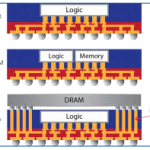
In constant pursuit of improved performance, power and cost, chip and system designers always want to integrate more functions together because this minimizes inter-device loads (affecting performance and power) and bill of materials on the board (affecting cost). However it generally isn’t possible to integrate … Read More
Processor cores come in a wide variety of speeds, performance and capabilities, so it may take you some time to find the proper processor for your system. Let’s say that you are designing a product for the industrial, automotive, military or medical markets that has an inherent requirement for safety, security and reliability… Read More
A few weeks back I wrote an article mentioning that Mentor Graphics has been quietly working on solutions for photonic integrated circuits (PICs) for some time now, while one of their competitors has recently established a photonics beachhead. One of the most common challenges for PIC designs is their curvilinear nature, thus… Read More
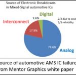
For decades, digital test has been fully automated including methodologies and automation for test pattern generation, grading and test time compression. Automation for analog and mixed-signal (AMS) IC test has not however kept pace. This is troubling as according to IBSapproximately 85% of SoC design starts are now AMS designs.… Read More
In the spectrum of functional verification platforms – software-based simulation, emulation and FPGA-based prototyping – it is generally agreed that while speed shoots up by orders of magnitude (going left to right) ease of debug drops as performance rises and setup time increases rapidly, from close to nothing for simulation… Read More
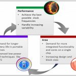
How to nail your PPA tradeoffsby Beth Martin on 11-03-2016 at 4:00 pmCategories: EDA, Siemens EDA
How do you ensure your design has been optimized for power, performance, and area? I posed this question to Mentor’s Group Director of Marketing, Sudhakar Jilla and product specialist Mark Le. They said that finding the PPA sweet spot is still often done by trial and error – basically serial experiments with various input parameters… Read More
In The Times They Are A Changin’ Nobel Laureate Bob Dylan advised us to “heed the call” of change or suffer the consequences. This couldn’t be more true, considering what design and verification engineers face every day in the midst of the technological revolution.
Change has never been so rapid. And it requires we constantly adapt.… Read More
Last Friday I learned something new about IoT by attending a SEMI event in Wilsonville, OR just a few short miles away from where I live in Tualatin. SEMI puts on two events here in Oregon each year, and their latest event on IoT Sensors was quite timely and popular judging by how many attendees showed up. First up was Jeff Miller from … Read More
IoT edge device design means four domains – MEMS, analog, digital, and RF – not only work together, but often live on the same die (or substrate in a 2.5D process) and are optimized for power and size. Getting these domains to work together effective calls for an enhanced flow.
Historically, these domains have not played together … Read More
Product lifecycle management is probably not the most gripping topic for most design engineers. You want to get on with architecture, design, verification and implementation. But if you are building products for any safety-sensitive application in a car, a medical appliance, avionics, railway applications in Europe – to name… Read More