You are currently viewing SemiWiki as a guest which gives you limited access to the site. To view blog comments and experience other SemiWiki features you must be a registered member. Registration is fast, simple, and absolutely free so please,
join our community today!
WP_Term Object
(
    [term_id] => 157
    [name] => EDA
    [slug] => eda
    [term_group] => 0
    [term_taxonomy_id] => 157
    [taxonomy] => category
    [description] => Electronic Design Automation
    [parent] => 0
    [count] => 4439
    [filter] => raw
    [cat_ID] => 157
    [category_count] => 4439
    [category_description] => Electronic Design Automation
    [cat_name] => EDA
    [category_nicename] => eda
    [category_parent] => 0
    [is_post] =>
)
Most designers are not using FinFETs yet, however the increased transistor density and power advantages they offer are compelling. Smaller feature sizes have been a consistent driver in semiconductor technology. Eventually the market will move more and more to FinFET processes, increasingly leaving behind planar transistors.… Read More
Since my blog about the Intel CEOs went over so well (sarcasm) I thought I should write more about semiconductor chief executive officers. This list comes from David Manners of Electronics Weekly who, unlike me, is a real journalist. Using David’s list as a starting point I will add more candidates at the end and please add yours in… Read More
Operational amplifiers, which are among the most widely used analog components found in nearly all types of electronic systems, are migrating toward zero-drift capability and much-greater range of voltages at the supplies and the inputs. Take Linear Technology Corp.’s LTC2057HV, a zero-drift operational amplifier, which… Read More
Digital designers are more numerous than analog IC designers, and so they tend to get more attention from EDA vendors in terms of tools and automation methodologies. For an analog design team with specialists focused separately on schematics and layout there are several methodology questions that need to be addressed, like:… Read More
At IEDM last week Coventor hosted a panel session as they do each year. The theme this year was surviving variation. The panel was hosted by someone whose name is familiar round here, Dan Nenni. The panel that Coventor had put together had people from all sorts of different slots in the design/supply chain for semiconductor. Unfortunately… Read More
Last VIP News of 2014by Eric Esteve on 12-22-2014 at 11:00 amCategories: IP, Synopsys
It’s likely that most of the current Semiwiki readers didn’t read this article posted in 2011, comparing Cadence and Synopsys with the Soviet Union and the USA, sharing the world in 1944 during the Yalta Conference. I was explaining in my post that Synopsys’s strong influence was on Design IP when Cadence’s preferred domain was … Read More
Results of TSMC’s ECO Fill Flowby Beth Martin on 12-22-2014 at 7:00 amCategories: EDA, TSMC
By Jeff Wilson, Mentor Graphics and Anderson Chiu, TSMC
At this year’s TSMC Open Innovation Platform® (OIP) Ecosystem Forum, Mentor Graphics and TSMC co-presented some results of the ECO Fill flow developed for TSMC customers working at advanced nodes. Here is a summary of the presentation. (TSMC customers can access the presentation… Read More
In today’s world where every device functions intelligently, it automatically becomes active on any kind of stimulus. The problem with such intelligence is that it can function unfavorably on any kind of bad stimulus. As the devices are complex enough in the form of SoCs (which at advanced process nodes are more susceptible to … Read More
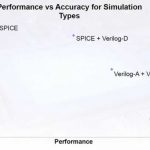
With advances in available IP, mixed signal design has become much easier. Mixed signal verification on the other hand is becoming more complicated. More complexity means more simulation, and in the analog domain, SPICE-based techniques grinding away on transistor models take a lot of precious time. Event-driven methods like… Read More
We’ve blogged dozens of times about UVM– Universal Verification Methodology at SemiWiki, and all of the major EDA vendors support UVM, so you may be lulled into thinking that UVM is totally adequate for top-down SoC verification. Yesterday I had a phone discussion with Frank Schirrmeister of Cadence about a new approach… Read More


Silicon Insurance: Why eFPGA is Cheaper Than a Respin — and Why It Matters in the Intel 18A Era