You are currently viewing SemiWiki as a guest which gives you limited access to the site. To view blog comments and experience other SemiWiki features you must be a registered member. Registration is fast, simple, and absolutely free so please,
join our community today!
WP_Term Object
(
    [term_id] => 157
    [name] => EDA
    [slug] => eda
    [term_group] => 0
    [term_taxonomy_id] => 157
    [taxonomy] => category
    [description] => Electronic Design Automation
    [parent] => 0
    [count] => 4441
    [filter] => raw
    [cat_ID] => 157
    [category_count] => 4441
    [category_description] => Electronic Design Automation
    [cat_name] => EDA
    [category_nicename] => eda
    [category_parent] => 0
    [is_post] =>
)
At this year’s SNUG (Synopsys Users Group) conference, Richard Ho, Head of Hardware, OpenAI, delivered the second keynote, titled “Scaling Compute for the Age of Intelligence.” In his presentation, Richard guided the audience through the transformative trends and implications of the intelligence era now unfolding before… Read More
LLMs are already simplifying assertion generation but still depend on human-generated natural language prompts. Can LLMs go further, drawing semantic guidance from the RTL and domain-specific training? Paul Cunningham (GM, Verification at Cadence), Raúl Camposano (Silicon Catalyst, entrepreneur, former Synopsys CTO… Read More
Modern vehicles have become quite sophisticated, like a supercomputer on wheels. They integrate a vast number of electronic components, including thousands of chips, to deliver advanced functionalities ranging from infotainment to critical safety systems. This increasing complexity necessitates a robust approach to … Read More
At the recent IPSoC Conference in Silicon Valley, Aparna Tarde gave a talk on the importance of Next-Gen Interconnects to scale AI infrastructure. Aparna is a Sr. Technical Product Manager at Synopsys. A synthesis of the salient points from her talk follows.
The rapid advancement of artificial intelligence (AI) is fundamentally… Read More
We all know semiconductor design is getting harder. Much harder when you consider the demands of AI workloads and heterogeneous integration of many chiplets in a single package. This class of system demands co-optimization across the entire design flow. For example, functional verification, thermal analysis, signal and power… Read More
The RISC-V ecosystem is witnessing remarkable growth, driven by increasing industry adoption and a thriving open-source community. As companies and developers seek customizable computing solutions, RISC-V has become a top choice. Providing a scalable and cost-effective ISA foundation, RISC-V enables high-performance… Read More
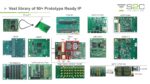
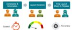
High-speed PCB designs are complex, often requiring a team with design engineers, PCB designers and SI/PI engineers working together to produce a reliable product, delivered on time and within budget. Cadence has been offering PCB tools for many years, and they recently wrote a 10-page white paper on this topic, so I’ll share … Read More
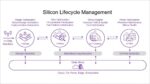
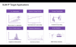
In an era defined by complex chip architectures, ever-shrinking technology nodes and very demanding applications, Silicon Lifecycle Management (SLM) has become a foundational strategy for optimizing performance, reliability, and efficiency across the lifespan of a semiconductor device. Central to effective SLM are Process,… Read More
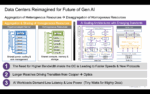
From my vantage point in the EDA foxhole it can be easy to forget that Cadence also has interests in much broader technology domains. One of these is in data center modeling and optimization, through their Cadence Reality Digital Twin Platform. This is an area in which they already have significant track record collaborating with… Read More
At NVIDIA’s recent GTC conference, a Cadence-NVIDIA joint session provided insights into how AI-powered innovation is reshaping the future of data center infrastructure. Led by Kourosh Nemati, Senior Data Center Cooling and Infrastructure Engineer from NVIDIA and Sherman Ikemoto, Sales Development Group Director from … Read More


Musk’s Orbital Compute Vision: TERAFAB and the End of the Terrestrial Data Center