You are currently viewing SemiWiki as a guest which gives you limited access to the site. To view blog comments and experience other SemiWiki features you must be a registered member. Registration is fast, simple, and absolutely free so please,
join our community today!
WP_Term Object
(
    [term_id] => 157
    [name] => EDA
    [slug] => eda
    [term_group] => 0
    [term_taxonomy_id] => 157
    [taxonomy] => category
    [description] => Electronic Design Automation
    [parent] => 0
    [count] => 4440
    [filter] => raw
    [cat_ID] => 157
    [category_count] => 4440
    [category_description] => Electronic Design Automation
    [cat_name] => EDA
    [category_nicename] => eda
    [category_parent] => 0
    [is_post] =>
)
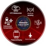
As a preferred carrier to data or energy, photonics technology is becoming broad and diverse. In IC design, silicon-photonics technology has been the enabler of new capabilities and has revolutionized many applications as Moore’s-based scaling started to experience a slowdown. It acts as new on-chip inductor in HPC design … Read More
As SoC and IP designs continue to increase in complexity while schedules accelerate, verification teams are looking for methodologies to improve design confidence more quickly. Formal verification techniques provide one route to improved design confidence, and the increase in papers and interest at industry conferences… Read More
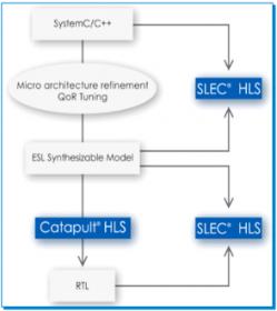
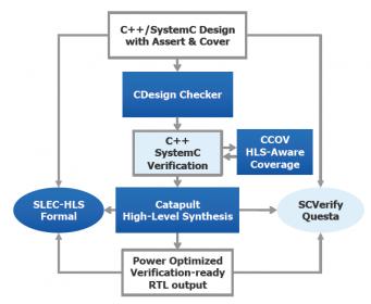
Higher level synthesis (HLS) of an IP block involves taking its high-level design specification –usually captured in SystemC or C++, synthesizes and generates its RTL equivalent. HLS provides a faster convergence path to design code stability, promotes design reuse and lowers front-end design inception cost.
HLS and Mentor… Read More
ANSYS recently hosted a webinar talking about how they used the big-data analytics available in RedHawk-SC to do early power grid planning with static analytics, providing better coverage than would have been possible through pure simulation-based approaches. The paradox here is that late-stage analysis of voltage drops … Read More
As 2018 wraps up this month it’s time to start thinking and planning for 2019, and if you work in the Silicon Valley then you’ll want to consider adding the 31st annual DVCon event planned for February 25-28 in San Jose. Surveys have shown for some time now that verification tasks actually take up more time on a SoC project… Read More
I met Imperas at TechCon this year because I wanted to become a bit more knowledgeable about virtual modeling. That led me to become more interested in RISC-V and a talk given by Krste Asanovic of UCB and SiFive. My takeaway surprised me. I had thought this was an open-source David versus proprietary Goliaths (Intel and ARM) battle… Read More
Cadence held a well-attended Automotive Summit where Cadence presented an overview of their solution and system enablement along with industry experts and established or startup companies sharing their perspective and product features from autonomous driving, LiDAR, Radar, thermal imaging, sensor imaging, and AI.… Read More
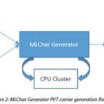
For SOC designers that are waiting for library models the saying “give me liberty or give me death” is especially apropos. Without libraries to support the timing flow, SOC design progress can grind to a halt. As is often the case, more than just a few PVT corners are needed. Years ago, corners were what the term sounded like – the 4 corners… Read More
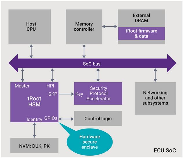
It used to be that automotive theft and crime was perpetrated with a crowbar. Now with increased electronics content, car designer and owners need to worry about electronic threats. Anywhere there is a communication link or a processor, there are potential threats to the security of the car. The range of these threats covers everything… Read More
In a recent whitepaper Gagandeep Singh, Director of Engineering at Mentor, a Siemens Business outlines a flow using Catapult Design Checker that helps in early detection of coding errors as many companies are turning to High-Level Synthesis (HLS) methodology. This requires that high -level C++ models are correct, that ambiguities… Read More


Musk’s Orbital Compute Vision: TERAFAB and the End of the Terrestrial Data Center