You are currently viewing SemiWiki as a guest which gives you limited access to the site. To view blog comments and experience other SemiWiki features you must be a registered member. Registration is fast, simple, and absolutely free so please,
join our community today!
Naveed Sherwani, President and CEO of SiFive, did the keynote for this year’s Silicon Summit. This is one of the premier events for the C level executives in Silicon Valley, absolutely. Naveed is one of the top visionaries for the semiconductor industry and he certainly did not disappoint this time or any other time in my experience.… Read More
SEMICON West and ES Design West are right around the corner here in San Francisco and I wanted to point out the Meet the Experts segment in the appropriately named Meet the Experts Theater. Great idea really and a super great line-up. The best part of course is actually meeting the experts. Over my 35 year semiconductor career I have… Read More
During my Taiwan visit, prior to Las Vegas, I was fortunate to spend time with Willy Chen and Vivian Jiang to prepare for the cloud panel I moderated at #56thDAC. Willy and Vivian are part of the ever-important Design Infrastructure Marketing Division of TSMC, which includes the internal and external cloud efforts. TSMC first announced… Read More
One of the perks of blogging on SemiWiki is the events you get to attend for FREE and the amazing people you get to meet and Wally Rhines is certainly one of those people. You will not find a more intelligent, innovative, and genuinely nice group of people in my experience. Having traveled the world meeting thousands of people I can tell… Read More
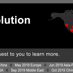
Join SiFive Tech Symposiums in Tokyo, Daejeon, Pangyo, Hsinchu, Singapore and Sydney
As we make our way around the world meeting and engaging with others in the semiconductor and hardware design community, we are seeing an increased interest in RISC-V based hardware innovation. This is due in large part to the emergence of market-ready… Read More
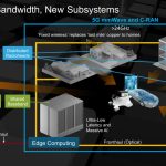
As much as I love all EDA vendors I must say Cadence did the best DAC this year. Great booth, great location, excellent content, and of course a great party. The 5G presentation in the Cadence booth by Ian Dennison was of great interest to me as I am still trying to wrap my head around this whole 5G thing. I was able to meet with Ian privately… Read More
Having just returned from my 35th DAC I would like to share a few thoughts with the organizers, exhibitors, and attendees. In my experience it was a really well planned DAC. Personally, I like the Las Vegas venue even though it is not near a semiconductor populated city. Those who chose to attend this year were there for a reason which… Read More
Probably the most interesting news out of 56thDAC thus far is the announcement that in 2020 and 2021 DAC will co-locate with SEMICON West. It’s great news really since this is something that has been discussed over the years but has been deadlocked due to “failed negotiations”. Unfortunately, simple logic goes out the window with… Read More
TSMC, the largest and most influential pure-play foundry, has many fascinating stories to tell. In this section, TSMC covers some of their basic history, and explains how creating an ecosystem of partners has been key to their success, and to the growth of the semiconductor industry.
The history of TSMC and its Open Innovation … Read More
eSilicon was one of the first companies to focus on making the benefits of the fabless semiconductor movement available to a broader range of customers and markets. The company is credited with the creation of the fabless ASIC model. In this section, eSilicon shares some of its history and provides its view of the ever-changing … Read More


Intel, Musk, and the Tweet That Launched a 1000 Ships on a Becalmed Sea