
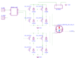
As systems become increasingly complex across every field of science and engineering, the importance of computer simulation in design, analysis, and verification continues to increase over time. The traditional process in which a system is modeled and simulated in a single tool is called monolithic simulation. On the other… Read More

Author: Admin
Enhancing Multi-Domain System Simulation with FMI Co-Simulation
GPU-native mask rule checking eliminates the curvilinear mask rule check bottleneck
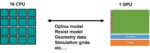
As semiconductor manufacturing pushes toward advanced nodes with tighter feature sizes, the optical proximity correction (OPC) workflow is adopting curvilinear masks to achieve the larger process windows that traditional Manhattan geometries cannot deliver.
Traditional Manhattan masks constrain shapes to vertical … Read More
John Barr: The EDA Veteran and Award-Winning Needham Funds Portfolio Manager

John Barr, Portfolio Manager of the top-ranked Needham Aggressive Growth Fund, has built a career with skills honed not just on Wall Street, but in the trenches of the early EDA industry.
Before becoming a respected sell-side analyst and later a buy-side portfolio manager, Barr spent 15 years in the EDA industry, working through… Read More
SoC PLANNER: A New Generation of SoC Design Exploration Solution Managing Cost-effectiveness and Sustainability
With over a trillion chips manufactured every year and application requirements evolving faster than ever (across automotive, HPC, and AI), the pressure on SoC design teams has never been higher with design space keeps growing and schedules keep shrinking.
Indeed, for a complex SoC project, the number of possible configurations… Read More
Crossing the Yield Cliff: IDP V6 and the Future of Manufacturing Forecasting
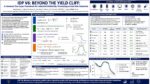
The paper, Industrial Defectivity Prediction (IDP) V6: A Two-Layer Yield Cliff Framework for Cross-Industry Mass-Production Forecasting, presents a generalized industrial yield-modeling architecture that extends the classical Negative Binomial framework through a two-layer phenomenological structure designed … Read More
Solving the EDA tool fragmentation crisis
By Samar Abd El-Hady and Wael ElManhawy
Design teams today face an uncomfortable truth: the specialized tools they need to verify modern ICs can’t reliably share the same design data. As geometries shrink below five nanometers and designs incorporate billions of transistors across multiple dies, no single Electronic… Read More
Carbon in the Age of AI Chips: What the Semiconductor Industry Needs to Know This Earth Day

Stephen Russell: Senior Technical Fellow, TechInsights
Every April, Earth Day prompts a flurry of corporate sustainability pledges and green-tinted press releases. But for the semiconductor industry in 2026, the conversation has moved well past pledges. Carbon accountability is now a procurement requirement, a regulatory… Read More
Speculation: Silicon’s Most Expensive Compulsion

How Time-Based Scheduling
Reclaims Silicon Wasted by Speculative Execution
By: Dr. Thang Tran, Founder and CTO, Simplex Micro
I have spent my career designing processor architectures, and I have reached an uncomfortable conclusion: a substantial fraction of the silicon area and power in modern high-performance processors… Read More
When a Platform Provider Becomes a Competitor: Why Arm’s Silicon Strategy Changes the Incentives

Marc Evans, Director of Business Development & Marketing, Andes Technology USA
I work at a RISC-V IP company, and I genuinely root for Arm — probably more than most people in my position would admit. Not because I’m confused about who competes with whom, but because Arm’s best move for their shareholders is also… Read More


Consolidation and Competition: Who is Winning the $4.5 Billion Interface IP Race?