 Generative AI is dramatically changing the compute power that must be delivered by advanced designs. This demand has risen by more than 10,000 times in the past five to six years. This increased demand has impacted the entire SoC design flow. We are now faced with going beyond 1 trillion transistors per chip, and systems now consist of many chips in a highly sophisticated package. Synopsys recently presented a webinar on these trends and offered some excellent strategies to tame the on-going demands of GenAI. A link to the replay is coming but first let’s examine some of the topics addressed in the Synopsys webinar detailing IP requirements for advanced AI chips.
You can access the webinar replay here.
About the Presenter

The webinar is presented by Dr. Manuel Mota, senior product manager responsible for the die-to-die interface IP product line at Synopsys. Manual has been with Synopsys for over 15 years. Previously, he held leadership roles at MIPS Technologies and Chipidea. He began his career as a researcher on microelectronics for high energy physics experiments at CERN, the European Organization for Nuclear Research.
Dr. Mota has authored multiple technical papers on multi-die design. He is clearly an expert in this area and the perfect person to present this webinar.
About the Webinar
Manuel begins the webinar with an overview of the impact generative AI has had on technology evolution. He shares many insights on the trends underway. The data is quite compelling. Here are just a few of the many items discussed:
- Larger compute chips
- Monolithic -> multi-die
- Advanced nodes for compute die
- Advanced packaging
- RDL interposers spanning multiple reticles
- 2D/2.5D -> 3D/3.5D
- Memory architectures
- cHBM, memory stacking
- Die-to-die bandwidth increasing
- 16G -> 32G -> 64Gbps/pin
Manuel then discusses SoC architectures that focus on higher compute performance. Included in this discussion are central I/O hub, homogeneous, cHBM extension and 3D stacking. Manuel then does a deep dive into three key technologies that show promise to deliver the required performance for multi-die designs.
1) Die-to-Die Communication
40/64G speeds can provide a 4X bandwidth advantage. Manuel discusses the standards that are driving increases in die-to-die communication. UCIe is a key driver here, and he spends some time explaining the various UCIe generations along with the benefits and challenges.
He then discusses Synopsys IP solutions for 64Gbps die-to-die communication. Key points here include:
- Lightweight implementation optimized for captive systems
- Differentiated feature set:
- Data rate up to 64Gbps/pin & low power modes and knobs
- Extensive testability, bring-up/debug & reliability functionality
- Lite FEC on link adapter for low latency error correction
- Modular architecture enables adaptation to system requirements
- Support streaming protocols
- Supports all package technologies (2D, 2.5D)
- Leverages Synopsys UCle 40G expertise & track record
Manuel gets into the details of how this IP is used in real world applications, with detailed information on technical capabilities and examples of delivered performance.
2) Custom HBMs
This approach can provide a 2X memory bandwidth advantage and more flexibility. Manual discusses some details of custom HBMs enabled with the logic process on the base die and how this opens the path for novel & efficient SoC memory architectures. He discusses the many benefits this approach offers. Some of the benefits covered include:
- Extend usage of HBM base die
- Multiple memory tiers reuse same die edge
- Offload some calculations to chiplet
- Isolates host from memory technology
- Extensible to other memory types
Manuel covers other benefits and strategies associated with this approach as well.
3) 3D Stacking
80% power savings are possible here, with an approach that delivers higher integration, shorter wiring and a more compact form factor. 3D stacking is clearly enabling the next generation of high performance SoCs. Manuel presents some commercial examples of this technology from Intel and AMD.
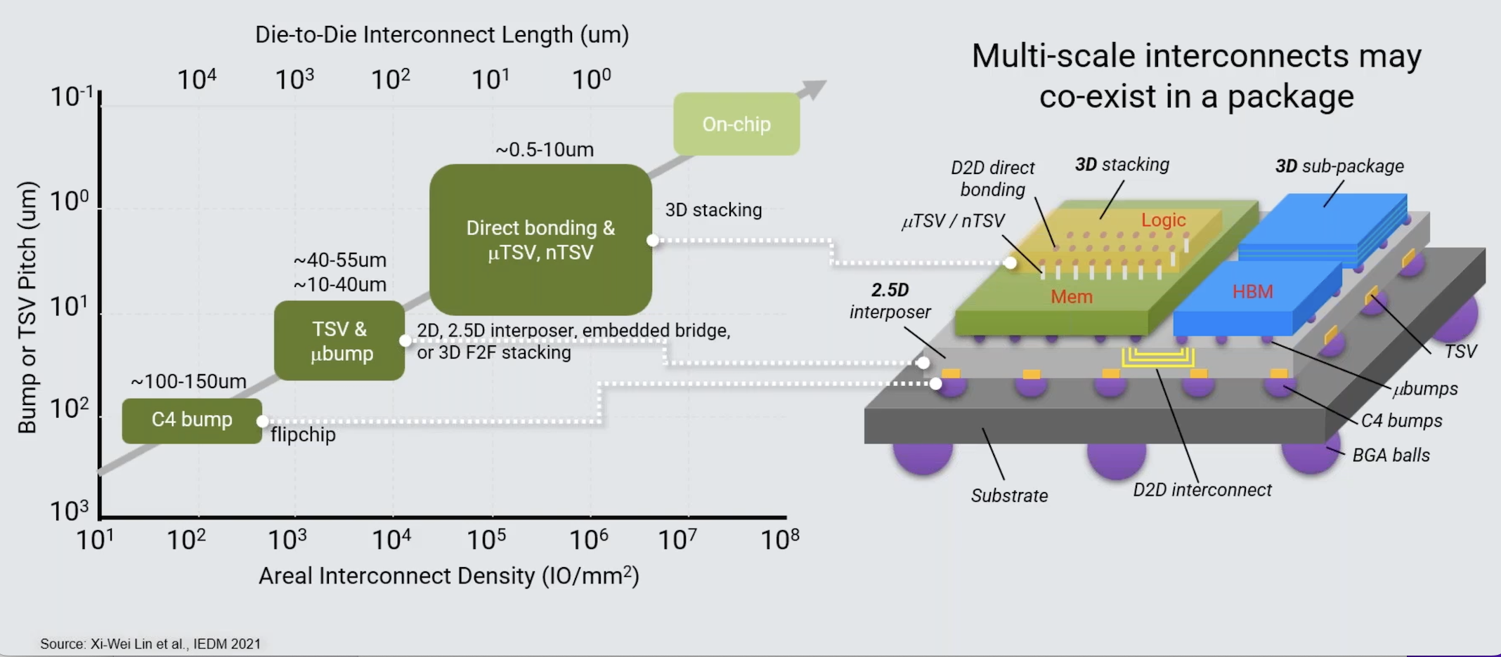
He dives into the architectural challenges that must be met to achieve a successful 3D implementation. Multi-die interconnect pitch scaling is a critical item here. He points out that shorter interconnects lead to lower die-to-die interface area/power/latency. Manual covers the details of several approaches for multi-die interconnect as summarized in the diagram below.

Multi-die assembly options from 2D to 3.5D are covered in detail. Manual also explores the design challenges and benefits of 3D stacking. Both face-to-back and face-to-face challenges and benefits are covered. How the various UCIe standards fit into each approach is also covered.
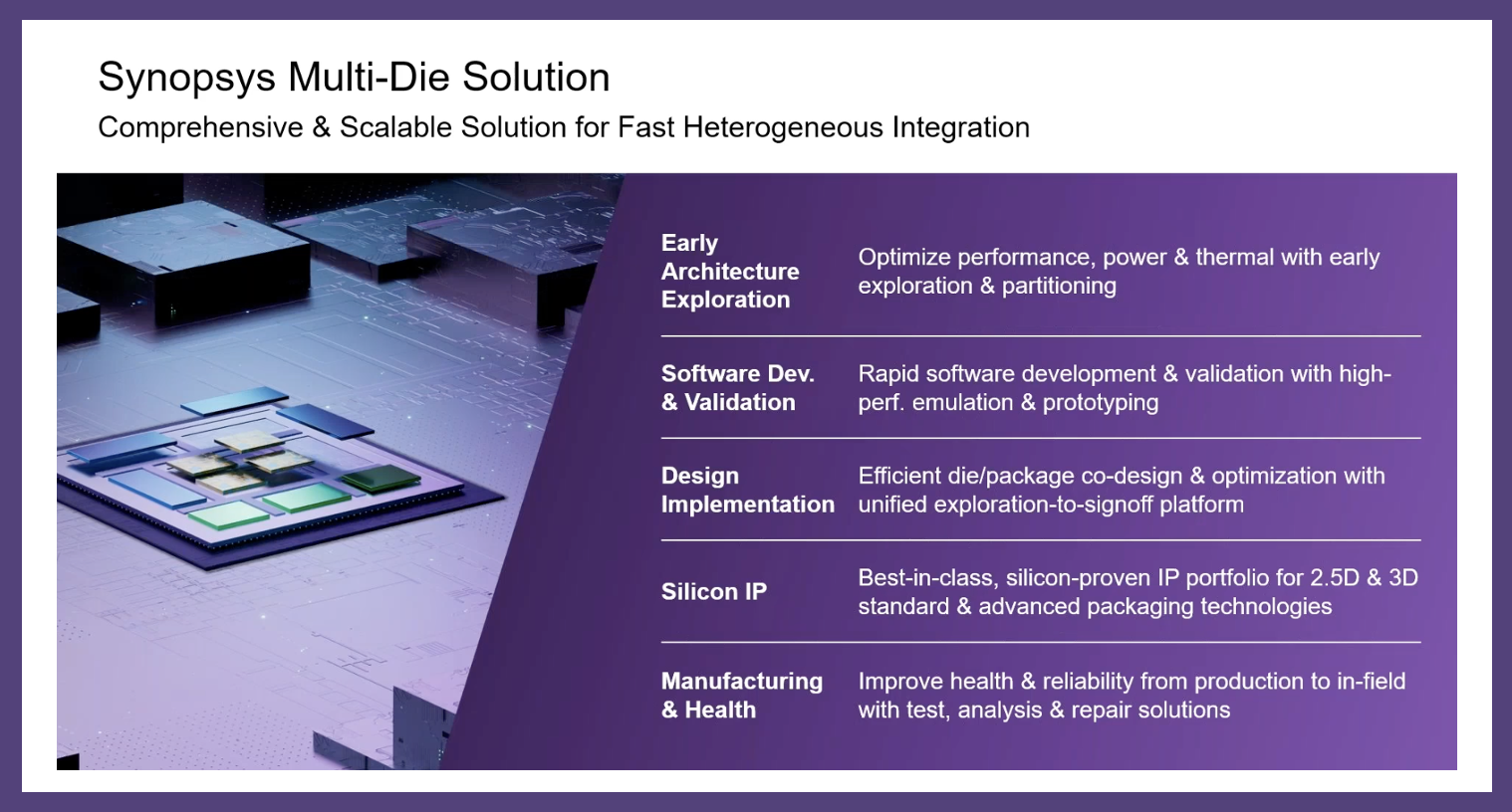
It’s clear that one approach doesn’t fit every project. Manuel spends some time explaining the various approaches that are available for multi-die implementation and how to choose the right one for your project. He concludes the webinar presentation with an overview of the comprehensive set of solutions that Synopsys provides to enable your journey to heterogeneous integration. A summary of this discussion is shown in the figure below.

The webinar concludes with an informative live Q&A session from audience questions.
To Learn More
It seems that every design team is feeling the power, performance and cost demands of advanced AI technology. If you are considering a multi-die approach, this webinar is a must-see event. Dr. Manuel Mota has deep experience with this type of design style, and he does a great job sharing ideas and technical approaches. You will learn something new. You can access the replay of the webinar here. And that’s how you can access the Synopsys webinar detailing IP requirements for advanced AI chips.
Also Read:
Synopsys Webinar: The Importance of Security in Multi-Die Designs – Navigating the Complex Landscape
Synopsys Executive Forum: Driving Silicon and Systems Engineering Innovation
Evolution of Memory Test and Repair: From Silicon Design to AI-Driven Architectures
Share this post via:


Comments
There are no comments yet.
You must register or log in to view/post comments.