GNSS is a wonderful invention, and low cost receivers have crept into smartphones and other mobile devices. However, GNSS does not solve all problems, especially in urban environments. The canyon effect blocks signals at street level between tall buildings, and signals do not penetrate to the interior of parking garages, tunnels,… Read More
How ST Designs with Layout Dependent Effects (LDE)
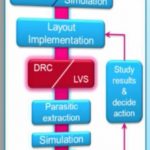
I first visited STat their Agrate, Italy site where Flash memory development is done. At DACthis year Antonio Bogani talked about how ST designs with LDE while using EDA tools and a PDK (Process Design Kit) from Cadence. They recorded the 17 minute presentation, and you can view it herewithout having to register. Antonio’s… Read More
WTL Leverage FDSOI to Achieve Both Low Power AND High Speed
In fact, this is the title of a presentation given by Pete Foley during FD-SOI Forum 2014 held in Shanghai, a couple of weeks ago. What is nice with clever people like Pete Foley is that they get the point, and get it quickly. Getting the point is to insert AND in capital in the title, as using FD-SOI technology allows to benefit from low-power… Read More
Design & EDA Collaboration Advances Mixed-Signal Verification through VCS AMS
Last week it was a rare opportunity for me to attend a webinar where an SoC design house, a leading IP provider and a leading EDA tool provider joined together to present on how the tool capabilities are being used for advanced mixed-signal simulation of large designs, faster with accuracy. It’s always been a struggle to combine design… Read More
A couple of misconceptions about FD-SOI
We have extensively discussed in Semiwiki about FD-SOI technology, explaining the main advantages (Faster, Cooler, Simpler), sometimes leading to very deep technical discussions, thanks to Semiwiki readers and their posts. I have recently found an article “Samsung & ST Team Up on 28nm FD-SOI”. This article includes many… Read More
FD-SOI at 14nm
At the recent Semicon West, Michel Haond of ST Microelectronics had a presentation on 14nm FD-SOI, or what they more lengthily call UTBB FD-SOI (which when you expand it all out comes to Ultra Thin Body and Buried-Oxide Fully Depleted Silicon on Insulator). When Chenming Hu (or whoever in his group) came up with the term FinFET it … Read More
When TSMC advocates FD-SOI…
I found a patent recently (May,14 2013) granted to TSMC “Planar Compatible FDSOI Design Architecture”, the following sentences, directly extracted from this patent, advertise FDSOI design better than a commercial promotion! “Devices formed on SOI substrates offer many advantages over their bulk counterparts, including… Read More
Analog Model Equivalence Checking Accelerates SoC Verification
In the race to reduce verification time for ever growing sizes of SoCs, various techniques are being adopted at different levels in the design chain, functional verification being of utmost priority. In an analog-digital mixed design, which is the case with most of the SoCs, the Spice simulation of analog components is the limiting… Read More
FD-SOI: 20nm Performance at 28nm Cost
There has been a lot of controversy about whether FD-SOI is or is not cheaper to manufacture than FinFET. Since right now FinFET is a 16nm process (22nm for Intel) and FD-SOI is, for now, a 28nm process it is not entirely clear how useful a comparison this is. Scotten Jones has very detailed process cost modeling software (that is what… Read More
Keywords: FD-SOI, Cost, FinFET
How to synthesize a pretty good article Is SOI Really Less Expensive, and even more important the impressive amount of comments (56) generated? Let’s start with the initial article. Pretty good, but slightly biased, when you carefully dissect it, like I did in one of the comments (you can find it in-extenso at the end of this post).… Read More