We all know semiconductor design is getting harder. Much harder when you consider the demands of AI workloads and heterogeneous integration of many chiplets in a single package. This class of system demands co-optimization across the entire design flow. For example, functional verification, thermal analysis, signal and power integrity, electromigration, and IR drop all need to be balanced across a complex process of die and package co-design. Data management and tool integration are particularly vexing here.
Against this backdrop, Siemens Digital Industries Software has published an eBook that flattens this class of problem. The company illustrates how its approach works using Intel Foundry’s EMIB packaging technology. If you face any type of complex chip design, this eBook is must-read. Don’t let the category scare you off, the eBook isn’t long, but It’s packed with solid examples of how to tame complex chip design. A link is coming but first let’s examine how Siemens describes its system-level prototyping and planning cockpit.
About the Authors
Two exceptional gentlemen with substantial background in the problems addressed in this eBook are the authors.

Keith Felton has over 30 years of experience developing and marketing advanced tools and supporting customers in the use of those tools for complex chip design, PCB design, and high-density advanced packaging. He has worked at companies such as Cadence, Viewlogic and Zuken-Redac as well as Siemens. He has also led partnerships across the semiconductor ecosystem.

Mike Walsh has over 30 years of experience helping customers around the world to design challenging advanced packages. He has broad knowledge of the system planning and design process and expertise in system-in-package (SiP), interposers, 3D IC, wafer-level integration, and multi-substrate solutions.
The insights offered by these authors is eye-opening, relevant and quite valuable.
About Intel Foundry’s EMIB Technology
Embedded multi-die interconnect bridge (EMIB) is a semiconductor packaging technology developed by Intel Foundry that uses a small, embedded silicon bridge to interconnect multiple dies, or chiplets, within a single package. In contrast to large silicon interposers, the EMIB bridge only spans the area needed to connect the specific dies, making it a more compact and cost-effective solution.
EMIB facilitates integration of multiple dies in a single package with the ability to have multiple EMIB bridges. This approach provides a good example of how to deploy an integrated chip/package flow since the increased design complexity intrinsic to EMIB technology shifts more of the challenges to the package level.
The Design Challenges
Design challenges include high pin counts, integration of diverse components, and providing an accurate representation of the EMIB structure for package design tools. Because EMIB is a passive bridge without active silicon, defining the EMIB component modules and setting up constraints to achieve low latency design rule checks (DRC) is crucial. Power delivery to the EMIB bridge is a primary design concern, requiring point-to-point connections and sufficient power distribution.
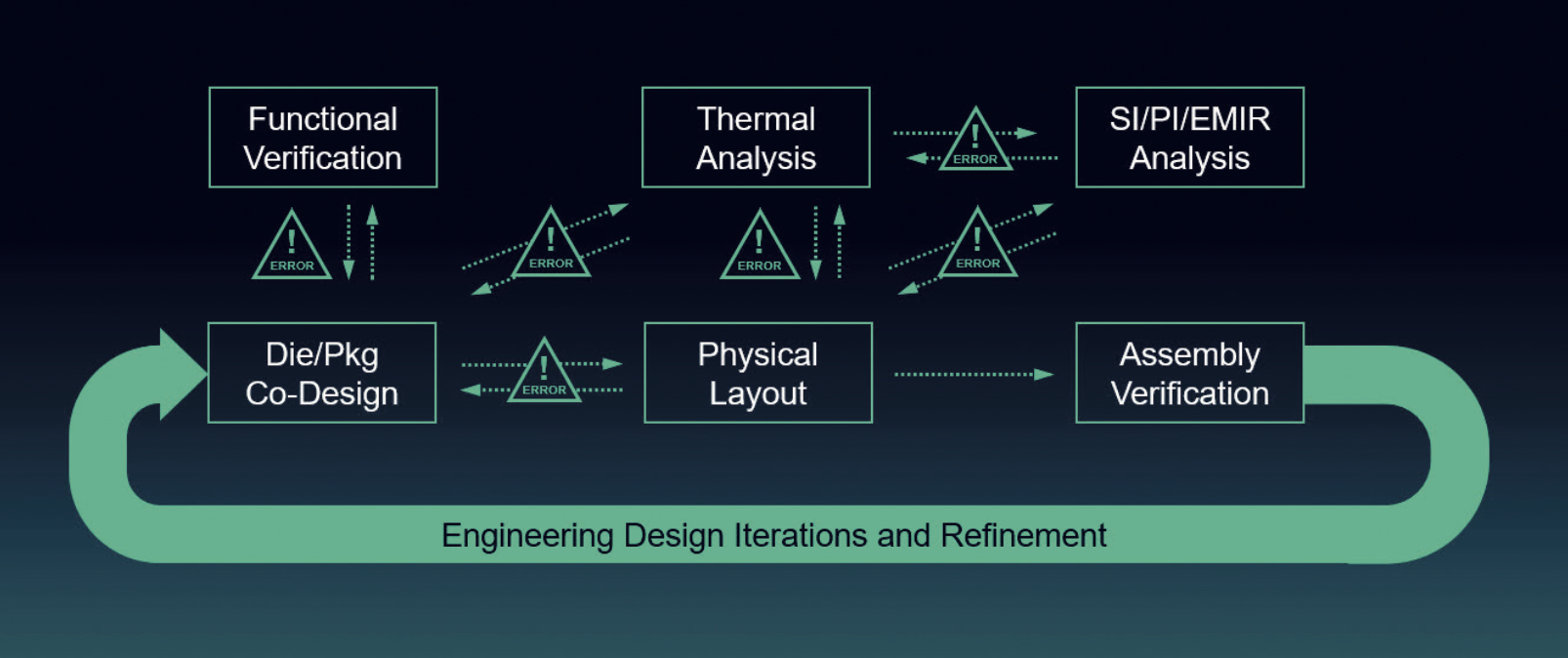
Typical advanced packaging workflows present several challenges. These flows include design and analysis tools from different vendors, creating disconnected manual processes. An environment like this requires importing and exporting a lot of data. This results in a lot of data iterations that can produce errors. This approach can also be time consuming, tempting designers to skip steps, such as functional simulation. But ignoring design steps results in failing to detect connectivity errors, producing non-functional designs.
The diagram below illustrates the complexity and interdependence of the process.

The Siemens System-Level Prototyping and Planning Cockpit
The eBook describes the Siemens approach to designing for Intel Foundry’s EMIB technology. This is accomplished by defining and driving everything from a single digital twin model of the entire advanced package assembly, which is constructed and managed by the Siemens Innovator3D IC™ solution.
Innovator3D IC uniquely represent the entire system, including dies, chiplets, interposers, EMIBs, packages, and PCBs within a single environment. It builds a cohesive view of the system by consuming data in a variety of formats and different levels of completeness. This unified view enables the creation of application-specific data sets, which are then pushed into other tools like Calibre® 3DSTACK, Calibre 3DThermal, Aprisa™, and Tessent™ from Siemens.
Innovator3D IC also leverages these tools in a predictive manner. For example, with Calibre 3DThermal, early insights into thermal performance can guide floor planning adjustments and corrective actions before serious issues arise. Even incomplete data, like preliminary power or heat sink information, can be used to overlay results back into Innovator3D IC providing valuable feedback for optimization.
By providing a platform that integrates all these tools and workflows, Innovator3D IC ensures early issue identification and seamless collaboration across the design flow, ultimately improving efficiency and design quality.
The eBook presents details of a six-step process to perform the complete, integrated design in one unified environment. The descriptions are clear and easy to follow. I highly recommend getting your copy of this eBook. The link is coming soon. The six steps detailed are:
- Step #1 – Die, EMIB, and package co-design
- Step #2 – Functional verification of system-level connectivity
- Step #3 – Early predictive thermal analysis
- Step #4 – Physical layout using Xpedition Package Designer
- Step #5 – SI/PI/EM analysis and extraction using HyperLynx
- Step #6 – 3D assembly verification using Calibre 3DSTACK
To Learn More
I have just scratched the surface of what you will learn from this Siemens eBook. If complex chip/package co-design is on your mind, and especially if you are considering Intel Foundry’s EMIB technology, you need to get your own copy.
You can access your copy of Reference workflows for Intel Foundry EMIB and MIB-T integration platforms here.
You can also learn more about the various tools from Siemens Digital Industries Software that comprise this unique and well-integrated flow here:
- Innovator3D IC
- Calibre 3DStack
- Calibre 3DThermal
- Aprisa SoC Design Software
- Xpedition Package Designer
- HyperLynx
- Tessent Silicon Lifecycle Solutions
And that’s how Siemens describes its system-level prototyping and planning cockpit.
Share this post via:


Comments
There are no comments yet.
You must register or log in to view/post comments.