As an engineer I’ve learned how to trade off using various EDA tools based on the accuracy requirements and the time available to complete a project. EDA vendors have been offering software tools to help us with reliability concerns like EM, IR drop and thermal analysis for several years now. Last week I attended a webinar from Silvaco that discussed how they have two approaches in this analysis area:
- Highest accuracy tool, used by circuit designers for sign-off – InVar
- Fastest run times, used by layout designers before design is LVS clean – InVar Prime
The InVar tools were part of an acquisition that Silvaco did of Invarian back in 2015, so it’s always a positive sign when the acquired product line continues to grow into new markets. With InVar Prime the tool user is the layout designer that wants to check out the quality of the routing and interconnect early on in the design process, even before the design is LVS clean. At such an early stage you can quickly pinpoint and fix the layout issues.
One technique to get fastest runs times for this type of analysis is to avoid using a SPICE circuit simulator, and instead use an approach with user-provided current source values. Here’s an overview of how this type of modeling works with an extracted IC layout:

A layout engineer can analyze the power and ground network for quality, estimate the IR drops, estimate current densities, look at point to point resistance values, uncover missing vias, find narrow wires and even uncover detour power routing. All of this early analysis will help meet the tape-out schedule and reduce costly design iterations.
So what does a user of InVar Prime have to supply the tool as inputs?
- GDSII or Open Access
- Technology file (ITF or iRCX)
- Current source info (from a GUI, script or SPICE results)
- Voltage source info
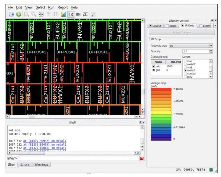
The capacity of InVar Prime is extended through the use of hierarchy, where each sub-block can be analyzed first before looking at the entire chip. Analysis speeds are quite fast, which allow the layout engineer to get multiple runs per day. Feedback from the analysis is both visually and textual, so for IR drop analysis you can see the regions of greatest drop in the color Red, or click on the text report to pinpoint the areas of greatest voltage drop:
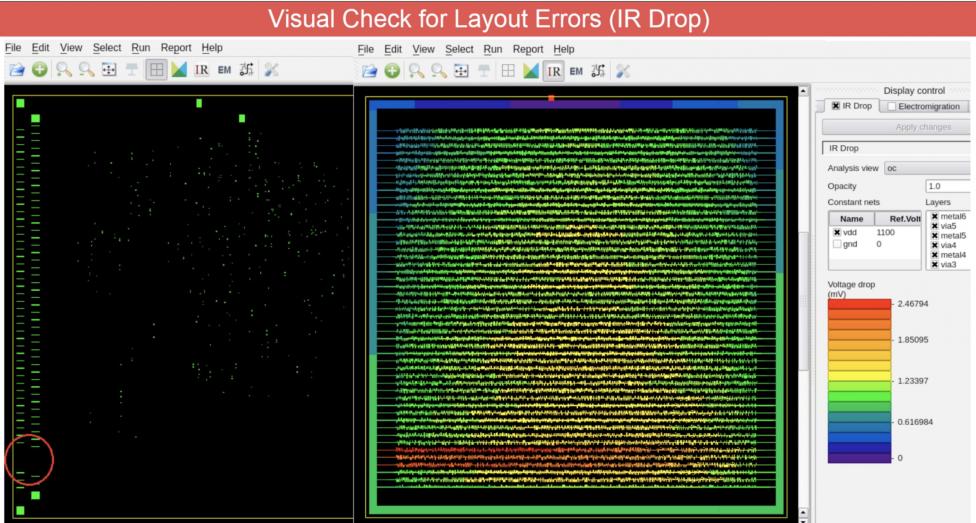
Using an example standard cell layout they introduced an error by removing vias in the power net at the lower-left corner, then ran the IR drop analysis to quickly show the regions of highest voltage drop:
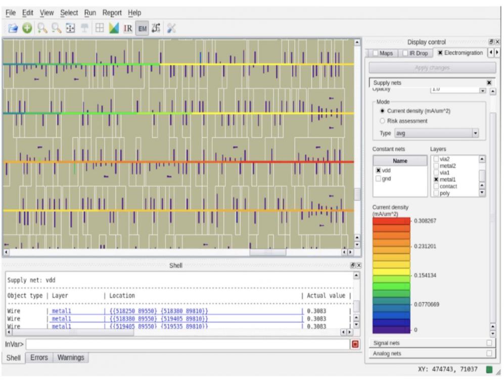
For EM and current density analysis your design can have any number of supply nets and you can see the regions of highest current density using the familiar rainbow of colors, review textual reports, or even click on a text report and view the graphical region. Scripting with the Tcl language can also be used to make your analysis even more automated.
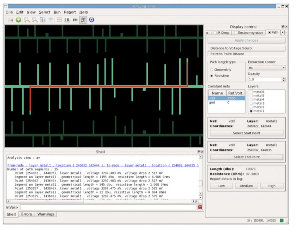
If you need to find where the greatest resistance is from the source of one point in your power network to its final destination then the analysis results are presented both visually and in text formats.
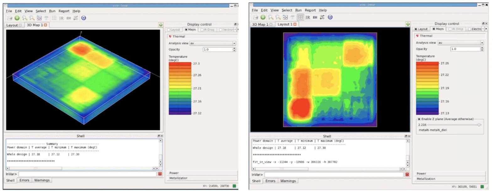
As an IC operates then each transistor produces heat based on the device sizes, currents, frequency and quality of the power and ground networks. The InVar Prime tool provides thermal analysis in either 2D or 3D modes.
It’s interesting to compare the faster speed of using InVar Prime (gold) versus the SPICE-based InVar tool on three different designs:
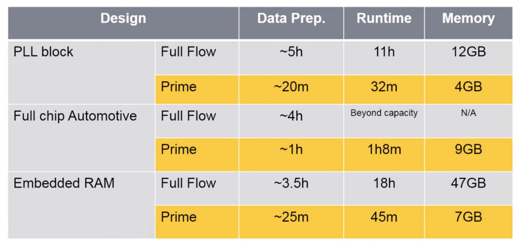
With InVar Prime the run times are faster, use less RAM and take less time to prepare the analysis.
Summary
IR, EM and thermal analysis are key to ensuring that your chip designs perform reliably and correctly in first silicon, so now you have two approaches from Silvaco with their InVar and InVar Prime tools. The InVar tool was introduced back in 2010 while the InVar Prime tool was introduced 12 months ago, and they have happy customers that have designed processors, displays, memories, high current IC, sensors, mobile, WiFi networks and wired network chips.
To view the archived webinar, watch it online.
Share this post via:

![SILVACO 051525 Webinar 400x400 v2[62]](https://semiwiki.com/wp-content/uploads/2025/04/SILVACO_051525_Webinar_400x400_v262.jpg)


Comments
There are no comments yet.
You must register or log in to view/post comments.