
Name: Tesla Dojo D1 Chip
Designed by: Tesla, Inc.
Announced: August 19, 2021 (AI Day)
First Deployment: 2023 (pilot systems), with full-scale training racks in 2024–2025
Fabricated by: TSMC
Process Node: N7 (D1 generation); future iterations expected on 5nm or 3nm
Use Case: Neural network training for autonomous vehicles and humanoid robotics
Architecture Type: Custom AI training ASIC with scalar, vector, and matrix execution units
Overview
The Tesla Dojo chip, known as the D1, is Tesla’s in-house AI training processor created to support its Full Self-Driving (FSD) vision system and robotics initiatives. Designed from the ground up, the chip enables massive-scale neural network training using vision data from millions of vehicles on the road. Dojo allows Tesla to break away from dependence on third-party GPUs (such as Nvidia), providing a vertically integrated AI compute platform.
Dojo is not a general-purpose processor—it’s purpose-built to optimize power efficiency, low-latency data exchange, and dense video-based training, which Tesla believes are essential for building real-world AI.
D1 Chip Technical Specifications
| Feature | Detail |
|---|---|
| Transistors | ~50 billion |
| Die Size | ~645 mm² |
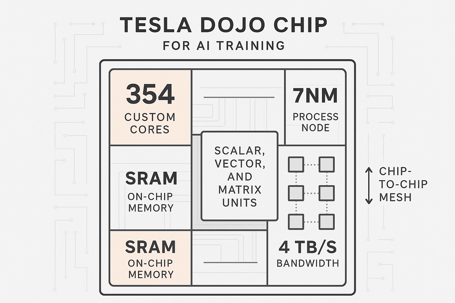
| Cores | 354 AI-optimized compute cores |
| Compute Style | Custom scalar, vector, and matrix units |
| Fabrication | TSMC 7nm process |
| I/O Bandwidth | 4 TB/s (mesh edge-to-edge) |
| SRAM | On-chip high-capacity SRAM (no HBM in v1) |
| Power Draw | ~400 watts per chip in full tile config |
| Instruction Set | Proprietary Tesla ISA |
| Interconnect | Direct chip-to-chip via proprietary high-bandwidth mesh |
Dojo scales up through modular tile-based compute systems:
Dojo Tile
-
25 D1 chips in a 5×5 mesh grid
-
~9 PFLOPs of FP16/BF16 performance per tile
-
Chips interconnected with edge-mesh routing
-
Designed for minimal communication latency
Rack and Exapod
-
10 tiles per tray, multiple trays per cabinet
-
Dojo cabinet includes power delivery, cooling, and switching
-
Dojo Exapod = 120+ tiles → 1+ ExaFLOP of compute (FP16)
Tesla envisions Dojo Exapods as AI factories for self-driving models, Tesla Bot (Optimus), and broader real-world AI applications.
Software Stack
-
Custom compiler and scheduler for Tesla’s AI workloads
-
Tensor and graph compilers optimized for Dojo ISA
-
End-to-end vertical integration: silicon → tile → compiler → data pipeline
Roadmap Timeline
| Year | Milestone |
|---|---|
| 2021 | Tesla AI Day unveils Dojo D1 |
| 2022 | First tiles validated |
| 2023 | Production-scale Dojo cabinets come online |
| 2024 | Multi-exapod systems deployed for FSD, robotics |
| 2025 | Expected D2 chip on 5nm or 3nm, potentially with HBM |
Strategic Importance
-
In-house training hardware accelerates AI development without Nvidia
-
Enables massive video dataset training for autonomy at lower cost
-
Supports AI model iteration speeds that Tesla claims outperform traditional cloud clusters
-
Platform for future humanoid robot training (Optimus)
Notable Quotes
“This is not a chip, it’s a training supercomputer in disguise.”
— Ganesh Venkataramanan, Tesla Dojo Project Leader (AI Day 2021)
“We’re using video-level data to train our models. That requires orders of magnitude more compute than tabular or text data. Dojo makes that possible.”
— Andrej Karpathy, Former Tesla Director of AI
“Dojo will be the fastest AI training computer in the world.”
— Elon Musk, Tesla Q3 2023 Earnings Call
“Dojo is optimized for bandwidth and scalability, not just peak FLOPs.”
— Pete Bannon, Tesla chip architect, ex-Apple PA Semi
“With Dojo, we’re building something that nobody else is building—we’re optimizing for the real world, not just benchmarks.”
— Elon Musk, Tesla AI Day 2021
“We built every part of Dojo ourselves—cores, interconnect, memory fabric, software. It’s Tesla silicon, end to end.”
Comparison with Nvidia and Google
| Feature | Tesla D1 (Dojo) | Nvidia H100 | Google TPU v5e |
|---|---|---|---|
| Process | TSMC N7 | TSMC N4 | TSMC N5 |
| Cores | 354 | 132 (Streaming Multiprocessors) | Unknown |
| Peak FP16 | ~362 TFLOPs (per chip) | 989 TFLOPs | ~400 TFLOPs |
| Interconnect | Mesh | NVLink | TPU interconnect |
| Memory | SRAM | HBM3 | HBM |
| Target Use | Vision AI, FSD | LLMs, GenAI | ML training/inference |


Chemical Origins of Environmental Modifications to MOR Lithographic Chemistry