

Also Known As: Embedded Memory IP, RAM/ROM IP, Non-Volatile Memory IP, eMemory IP
Domain: Semiconductor Design, System-on-Chip (SoC), Embedded Systems
Overview
Memory IP refers to pre-designed and verified memory blocks that can be integrated into larger semiconductor chips such as SoCs (System-on-Chips), ASICs, and FPGAs. These reusable components support data storage, caching, buffering, or program memory, and include various types like SRAM, DRAM, ROM, EEPROM, Flash, and emerging non-volatile memory (NVM) technologies.
Memory IP accelerates chip design by offering ready-to-use, silicon-proven modules optimized for area, power, and performance, while also ensuring compatibility with the target manufacturing process node.
Types of Memory IP
1. Volatile Memory IP
-
SRAM (Static RAM)
-
Used for cache, registers, and high-speed temporary storage.
-
Fast access, high power, and large area.
-
Common in CPUs, GPUs, and network processors.
-
-
DRAM (Dynamic RAM)
-
Higher density, lower cost per bit than SRAM.
-
Rarely embedded due to complexity; usually off-chip.
-
-
Register Files
-
Custom SRAM-like blocks for CPU register storage or buffering.
-
Often used in DSPs and tightly-coupled compute blocks.
-
2. Non-Volatile Memory (NVM) IP
-
ROM (Read-Only Memory)
-
Fixed data (e.g., bootloaders, device IDs).
-
One-time programmable (OTP).
-
-
Flash Memory
-
Electrically erasable and programmable.
-
Useful for embedded firmware, microcontroller code, and secure data.
-
-
EEPROM
-
Electrically erasable but slower and more expensive than Flash.
-
Often used in embedded configuration data.
-
-
Fuse/Antifuse/OTP
-
Used for configuration bits, encryption keys, hardware IDs.
-
-
Emerging NVM IP
-
ReRAM (Resistive RAM), MRAM (Magnetoresistive RAM), FRAM (Ferroelectric RAM), PCM (Phase-Change Memory).
-
Promise faster access, higher endurance, or radiation hardness.
-
Supplied by companies like Weebit Nano, Avalanche, and Everspin.
-
Key Functions and Use Cases
| Use Case | Memory Type | Application Examples |
|---|---|---|
| CPU cache | SRAM | L1/L2 cache in microprocessors |
| Program code storage | Flash, ROM | Embedded firmware, secure boot |
| Key storage | OTP, Fuse, PUF | Hardware root of trust, secure elements |
| Lookup/storage tables | SRAM, CAM, DRAM | Networking, AI accelerators, image processors |
| Configuration data | EEPROM, ReRAM | IoT, automotive ECUs |
IP Providers and Ecosystem
| Vendor | Specialty |
|---|---|
| Arm | Embedded SRAM/ROM (via Artisan Physical IP) |
| Synopsys | SRAM, ROM, NVM, OTP (DesignWare IP) |
| eMemory | OTP, NeoFuse, NeoPUF (widely used in TSMC flows) |
| Kilopass | Logic-compatible OTP and antifuse IP |
| Weebit Nano | ReRAM (emerging NVM) |
| MoSys | High-speed embedded memory IP (now Peraso) |
| SureCore | Low-power SRAM IP |
| Sidense (acq. by Synopsys) | One-Time Programmable IP |
| Menta | Embedded FPGA IP with embedded RAM |
Integration Considerations
-
Process Technology Compatibility
Memory IP must be optimized for each process node (e.g., TSMC N7, GF 22FDX, Intel 18A). -
Power, Area, Performance (PPA)
Trade-offs among size, latency, and leakage must be balanced for target applications. -
Error Correction (ECC)
Embedded memories in automotive, aerospace, or safety-critical applications often require ECC or parity logic. -
Security
Secure memories for encryption keys may require special shielding, tamper detection, or PUFs (Physically Unclonable Functions). -
Test and Repair
Many memory IP blocks come with built-in self-test (BIST) and redundancy for yield improvement.
Trends in Memory IP
-
AI and ML acceleration: Drives need for high-speed, low-latency on-chip SRAM and CAMs.
-
Automotive and IoT: Push for low-power NVM (e.g., ReRAM, MRAM) for edge computing.
-
Security and Trust: Demand for secure memory IP with PUF, OTP, and logic-based keys.
-
3D IC and Chiplets: Embedded memories used in interposer or chiplet-level architectures.
-
Process Scaling Challenges: Beyond 5nm, SRAM scaling becomes harder; emerging memories fill the gap.
Conclusion
Memory IP is a foundational building block in chip design, enabling fast, efficient, and secure data storage. With process portability, silicon validation, and customizability, memory IP accelerates product development while reducing risk. As emerging workloads demand more intelligent and secure memory behavior, innovation in this space—particularly in low-power SRAM, ReRAM, and PUF-enabled IP—continues to grow rapidly.
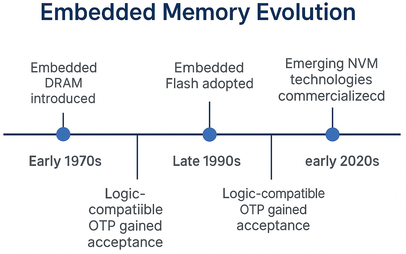
📜 Timeline: Embedded Memory Evolution
1970s – Early Embedded Memories
-
Mask ROM (MROM) and PROM are first embedded memories.
-
Used primarily in calculators, simple control chips.
-
Limited flexibility; data burned at fabrication.
1980s – Introduction of SRAM
-
SRAM (Static RAM) becomes standard for cache and register storage.
-
DRAM used externally; not yet viable for embedding.
-
Custom SRAM blocks in ASICs and early microcontrollers.
1990s – Embedded Flash & EEPROM
-
EEPROM and Flash IP integrated in microcontrollers.
-
Enables rewritable program storage on-chip.
-
Used in early consumer electronics and automotive ECUs.
2000s – OTP, Antifuse, and Security Memory IP
-
One-Time Programmable (OTP) memories rise in popularity.
-
Start of fuse/antifuse for ID, configuration, and secure keys.
-
Companies like eMemory and Kilopass emerge.
2010s – Low Power and Specialty SRAM
-
Demand for low-power SRAM in mobile, IoT, and wearables.
-
Secure memory IP grows: PUF (Physically Unclonable Functions), TRNG (True Random Number Generator).
-
Embedded memory for AI starts with CAM and high-speed SRAM.
Late 2010s – Emerging Non-Volatile Memories (NVM)
-
Research into ReRAM, MRAM, FRAM, and PCM.
-
Initial IP licensing from startups like Weebit Nano, Avalanche, and Everspin.
-
Used in harsh environments and battery-backed systems.
2020s – AI & Chiplet-Driven Memory
-
In-memory compute, large SRAM buffers for AI accelerators.
-
Growth of eNVM IP for secure edge AI and automotive (ASIL-D).
-
Memory IP optimized for chiplets, 2.5D/3D ICs, and heterogenous integration.
-
ReRAM and MRAM begin volume adoption.
Future Trends (late 2020s – 2030s)
-
Universal Memory: hybrid SRAM + NVM behavior (fast, dense, low power).
-
Radiation-hardened memory IP for aerospace.
-
AI-managed memory hierarchy inside SoCs.


CEO Interview with Jerome Paye of TAU Systems