High Bandwidth Memory (HBM) Wiki

Published by Admin on 04-07-2020 at 12:24 pm
Last updated on 07-08-2020 at 12:25 pm

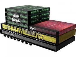
High Bandwidth Memory (HBM) is a high-performance RAM interface for 3D-stacked SDRAM from Samsung, AMD and SK Hynix. It is used in conjunction with high-performance graphics accelerators and network devices. The first HBM memory chip was produced by SK Hynix in 2013, and the first devices to use HBM were the AMD Fiji GPUs in 2015.

High Bandwidth Memory has been adopted by JEDEC as an industry standard in October 2013. The second generation, HBM2, was accepted by JEDEC in January 2016.

Technology

HBM achieves higher bandwidth while using less power in a substantially smaller form factor than DDR4 or GDDR5. This is achieved by stacking up to eight DRAM dies (thus being a Three-dimensional integrated circuit), including an optional base die with a memory controller, which are interconnected by through-silicon vias (TSVs) and microbumps. The HBM technology is similar in principle but incompatible with the Hybrid Memory Cube interface developed by Micron Technology.

HBM memory bus is very wide in comparison to other DRAM memories such as DDR4 or GDDR5. An HBM stack of four DRAM dies (4‑Hi) has two 128‑bit channels per die for a total of 8 channels and a width of 1024 bits in total. A graphics card/GPU with four 4‑Hi HBM stacks would therefore have a memory bus with a width of 4096 bits. In comparison, the bus width of GDDR memories is 32 bits, with 16 channels for a graphics card with a 512‑bit memory interface. HBM supports up to 4 GB per package.

The larger number of connections to the memory, relative to DDR4 or GDDR5, required a new method of connecting the HBM memory to the GPU (or other processor). AMD and Nvidia have both used purpose-built silicon chips, called interposers, to connect the memory and GPU. This interposer has the added advantage of requiring the memory and processor to be physically close, decreasing memory paths. However, as semiconductor device fabrication is significantly more expensive than printed circuit board manufacture, this adds cost to the final product.

Interface

The HBM DRAM is tightly coupled to the host compute die with a distributed interface. The interface is divided into independent channels. The channels are completely independent of one another and are not necessarily synchronous to each other. The HBM DRAM uses a wide-interface architecture to achieve high-speed, low-power operation. The HBM DRAM uses a 500 MHz differential clock CK_t / CK_c (where the suffix “_t” denotes the “true”, or “positive”, component of the differential pair, and “_c” stands for the “complementary” one). Commands are registered at the rising edge of CK_t, CK_c. Each channel interface maintains a 128‑bit data bus operating at double data rate (DDR). HBM supports transfer rates of 1 GT/s per pin (transferring 1 bit), yielding an overall package bandwidth of 128 GB/s.

HBM2

The second generation of High Bandwidth Memory, HBM2, also specifies up to eight dies per stack and doubles pin transfer rates up to 2 GT/s. Retaining 1024‑bit wide access, HBM2 is able to reach 256 GB/s memory bandwidth per package. The HBM2 spec allows up to 8 GB per package. HBM2 is predicted to be especially useful for performance-sensitive consumer applications such as virtual reality.

On January 19, 2016, Samsung announced early mass production of HBM2, at up to 8 GB per stack. SK Hynix also announced availability of 4 GB stacks in August 2016.

NEC SX-Aurora TSUBASA uses HBM 2

HBM2E

In late 2018, JEDEC announced an update to the HBM2 specification, providing for increased bandwidth and capacities. Up to 307 GB/s per stack (2.5 Tbit/s effective data rate) is now supported in the official specification, though products operating at this speed had already been available. Additionally, the update added support for 12‑Hi stacks (12 dies) making capacities of up to 24 GB per stack possible.

On March 20, 2019, Samsung announced their Flashbolt HBM2E, featuring eight dies per stack, a transfer rate of 3.2 GT/s, providing a total of 16 GB and 410 GB/s per stack.

August 12, 2019, SK Hynix announced their HBM2E, featuring eight dies per stack, a transfer rate of 3.6 GT/s, providing a total of 16 GB and 460 GB/s per stack. SK Hynix will begin mass production in 2020.

DesignWare HBM IP Solution

Advanced graphics, high-performance computing (HPC) and networking applications are requiring more memory bandwidth to keep pace with the increasing compute performance brought by advanced process technologies. With the DesignWare HBM2/HBM2E IP solution, designers can achieve their memory throughput requirements with minimal power consumption and low latency.

The complete DesignWare HBM2/HBM2E IP solution includes controller, PHY and verification IP, enabling designers to achieve up to 409 GBps aggregate bandwidth, which is over 14 times the bandwidth of a 72-bit DDR4 interface operating at 3200 Mbps. In addition, the DesignWare HBM2/HBM2E IP solution delivers approximately 10X better energy efficiency than DDR4.

The DesignWare HBM2/HBM2E IP solution leverages elements from Synopsys’ silicon-proven DDR4 IP, which has been validated in hundreds of designs and shipped in millions of systems-on-chips (SoCs), enabling designers to lower integration risk and accelerate adoption of the new standard. In addition, DesignWare HBM IP is in volume production with numerous customer SoCs.

The DesignWare HBM2/HBM2E PHY is provided as a set of hard macrocells delivered as GDSII along with a soft PHY Utility Block (PUB). The hard macrocells include integrated application-specific HBM2/HBM2E I/Os required for HBM2/HBM2E signaling and are easily assembled into a complete 512- or 1,024-bit HBM2/HBM2E PHY. The PUB provides the PHY configuration registers, training algorithms, and BIST features of the interface. The design is optimized for high performance, low latency, low area, low power, and ease of integration.

DesignWare HBM2 PHY IP block diagram

Figure 1: DesignWare HBM2/HBM2E PHY IP Block Diagram

History

Die-stacked memory was initially commercialized in the flash memory industry. Toshiba introduced a NAND flash memory chip with eight stacked dies in April 2007, followed by Hynix Semiconductor introducing a NAND flash chip with 24 stacked dies in September 2007.

3D-stacked random-access memory (RAM) using through-silicon via (TSV) technology was commercialized by Elpida Memory, which developed the first 8 GB DRAM chip (stacked with four DDR3 SDRAM dies) in September 2009, and released it in June 2011. In 2011, SK Hynix introduced 16 GB DDR3 memory (40 nm class) using TSV technology, Samsung Electronics introduced 3D-stacked 32 GB DDR3 (30 nm class) based on TSV in September, and then Samsung and Micron Technology announced TSV-based Hybrid Memory Cube (HMC) technology in October.

Development

The development of High Bandwidth Memory began at AMD in 2008 to solve the problem of ever-increasing power usage and form factor of computer memory. Over the next several years, AMD developed procedures to solve die-stacking problems with a team led by Senior AMD Fellow Bryan Black. To help AMD realize their vision of HBM, they enlisted partners from the memory industry, particularly Korean company SK Hynix, which had prior experience with 3D-stacked memory, as well as partners from the interposer industry (Taiwanese company UMC) and packaging industry (Amkor Technology and ASE).

AMD Fiji, the first GPU to use HBM

The development of HBM was completed in 2013, when SK Hynix built the first HBM memory chip. HBM was adopted as industry standard JESD235 by JEDEC in October 2013, following a proposal by AMD and SK Hynix in 2010. High volume manufacturing began at a Hynix facility in Icheon, South Korea, in 2015.

The first GPU utilizing HBM is AMD Fiji which was released in June 2015 powering the AMD Radeon R9 Fury X.

In January 2016, Samsung Electronics began early mass production of HBM2. The same month, HBM2 was accepted by JEDEC as standard JESD235a. The first GPU chip utilizing HBM2 is the Nvidia Tesla P100 which was officially announced in April 2016.

Future

At Hot Chips in August 2016, both Samsung and Hynix announced the next generation HBM memory technologies. Both companies announced high performance products expected to have increased density, increased bandwidth, and lower power consumption. Samsung also announced a lower-cost version of HBM under development targeting mass markets. Removing the buffer die and decreasing the number of TSVs lowers cost, though at the expense of a decreased overall bandwidth (200 GB/s).

References:

https://www.synopsys.com/dw/ipdir.php?ds=dwc_hbm2

https://en.wikipedia.org/wiki/High_Bandwidth_Memory

Share this post via:

Comments

There are no comments yet.

You must register or log in to view/post comments.