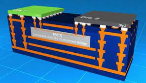
EMIB (Embedded Multi-die Interconnect Bridge) is an advanced 2.5D packaging technology developed by Intel that enables high-density, high-bandwidth, low-latency interconnects between chiplets (dies) within a single package—without requiring a full silicon interposer. EMIB offers a modular and scalable approach to heterogeneous integration, supporting CPUs, GPUs, memory (e.g., HBM), and accelerators in high-performance systems.
Introduced in 2014 and first used commercially in 2018 (in Intel’s Kaby Lake-G platform), EMIB is now a key part of Intel’s IDM 2.0 strategy and Intel Foundry Services (IFS) advanced packaging portfolio, often combined with other technologies like Foveros (3D stacking) and ODI (Omni-Directional Interconnect).
Overview
EMIB allows different dies to communicate efficiently within a single package using a small silicon bridge embedded into the package substrate. This bridge provides fine-pitch connections between adjacent dies—without the cost and complexity of a full silicon interposer used in traditional 2.5D solutions like TSMC CoWoS or Samsung I-Cube.
The EMIB bridge sits beneath the chiplets and offers short, dense interconnects for high-bandwidth, low-power, and high-yield integration.
Key Features
| Feature | Description |
|---|---|
| 2.5D Integration | Side-by-side die placement with localized interconnect |
| Embedded Bridge | Small silicon die embedded in the package substrate |
| High Interconnect Density | Fine-pitch micro-bump connections |
| No Full Interposer | Avoids large, costly silicon interposers |
| Heterogeneous Integration | Combines dies from different nodes, fabs, and functions |
| Flexible Design | Supports mix-and-match chiplets, scalable system design |
How EMIB Works
-
A small silicon bridge (~a few mm wide) is embedded into the organic package substrate during manufacturing.
-
Two or more adjacent chiplets (e.g., CPU + GPU, CPU + HBM) are placed over the substrate, aligning with the EMIB.
-
Each die connects to the EMIB through micro-bumps, creating a dense, short interconnect path across dies.
-
High-speed signals, clocking, and power distribution traverse the bridge.
-
There is no need for TSVs (through-silicon vias) or a large interposer wafer.
Advantages of EMIB
-
Lower Cost: Avoids the expense of a full interposer wafer.
-
Smaller Footprint: More compact than interposer-based designs.
-
Better Thermal Management: Improved heat dissipation vs. stacked dies.
-
High Bandwidth: Comparable to 2.5D silicon interposer designs.
-
Modularity: Easier to upgrade or customize individual chiplets.
-
Yield Benefits: Improves yield by integrating known-good dies (KGD).
Applications
EMIB is used in a variety of high-performance and modular products:
Intel Products:
-
Kaby Lake-G (Intel CPU + AMD Vega GPU + HBM2 via EMIB)
-
Intel Stratix 10 FPGA (logic + transceivers via EMIB)
-
Ponte Vecchio (Xe HPC GPU with over 47 chiplets)
-
Meteor Lake (Modular client SoC combining CPU, GPU, SoC dies)
-
Falcon Shores (future XPU architecture for AI/HPC)
IFS & Partner Projects:
-
Intel offers EMIB to foundry customers via Intel Foundry Services
-
Can be combined with UCIe for standardized die-to-die communication
EMIB vs. Other Packaging Technologies
| Feature | EMIB | TSMC CoWoS | Intel Foveros | Samsung I-Cube |
|---|---|---|---|---|
| Type | 2.5D | 2.5D | 3D | 2.5D |
| Interposer | Embedded bridge | Full silicon | Die stacking | Interposer |
| TSVs | No | Yes | Yes | Yes |
| Memory Integration | Yes (HBM) | Yes | Yes | Yes |
| 3D Stacking | No | No | Yes | No |
| Cost | Lower | Higher | Medium–High | Medium |
EMIB + Foveros: Intel’s Advanced Packaging Stack
Intel often combines EMIB and Foveros in a single design:
-
EMIB: For horizontal, high-bandwidth die-to-die links (e.g., HBM integration, GPU+GPU, SoC+I/O)
-
Foveros: For vertical stacking of logic on logic (CPU-on-SoC, cache-on-CPU)
This hybrid approach powers products like Ponte Vecchio and enables modular SoC disaggregation with heterogeneous integration.
EMIB and UCIe
Intel is a founding member of the UCIe (Universal Chiplet Interconnect Express) consortium. EMIB serves as a physical interconnect fabric in Intel’s chiplet ecosystem, and it supports UCIe-based communication for standardization across chiplet providers.
Challenges
-
Precision Alignment: Requires accurate die placement over small bridges
-
Design Complexity: Needs co-design between silicon, bridge, and substrate
-
Thermal Isolation: Must manage heat between adjacent high-power dies
-
EDA Tooling: Integration flows differ from conventional SoC designs
Future Directions
-
EMIB roadmap includes higher lane speeds, greater link density, and larger bridge arrays
-
ODI (Omni-Directional Interconnect) extends EMIB to support vertical and horizontal connectivity
-
Next-gen HBM4 and multi-tile AI accelerators will further drive EMIB adoption
-
Intel Foundry Services (IFS) is building EMIB into its open packaging ecosystem for external customers
Also Read:
3D IC (Three-Dimensional Integrated Circuit) Wiki
IC Packaging Comparison Wiki (TSMC, Intel, Samsung)
Intel 18A Process Technology Wiki
Intel Backside Power Delivery (PowerVia) Wiki
Share this post via:


Captain America: Can Elon Musk Save America’s Chip Manufacturing Industry?