
 SemiWiki")
Backside Power Delivery (BSPD), also called Backside Power Delivery Network (BSPDN) or backside power via (BPV) technology, is a semiconductor manufacturing innovation in which the chip’s primary power distribution network is relocated from the front side (transistor and signal interconnect layers) to the backside of the wafer.
This approach enables more efficient power delivery, reduces routing congestion, and improves performance, power efficiency, and scalability—especially for advanced nodes at 2nm and beyond.
Overview
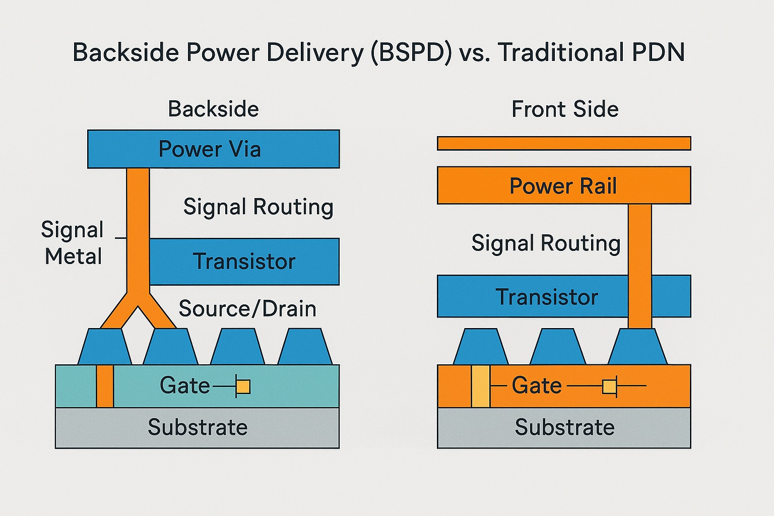
In traditional semiconductor design, both power rails and signal routing are implemented in the front-side metal layers above the transistor layer. As feature sizes shrink and transistor density increases, these routing layers become congested, creating resistance and capacitance bottlenecks.
BSPD separates power and signal networks by delivering power directly from the backside of the wafer through backside vias (sometimes called power vias) that connect to buried power rails near the transistor layer.
Signal routing remains entirely on the front side, which frees up metal tracks, shortens signal paths, and reduces delay.
Key Technical Benefits
-
Reduced IR Drop:
Power travels through shorter, thicker metal paths from backside to transistor, lowering voltage drop and allowing higher and more stable operating frequencies. -
Freed Front-Side Routing:
With power lines moved to the backside, more front-side routing tracks are available for signals, reducing congestion and wire length. -
Improved Power Efficiency:
Lower resistance in the PDN and reduced signal wire capacitance lower overall power consumption (both static and dynamic). -
Better Power Integrity:
Lower voltage noise (droop) allows for reduced voltage guardbands, improving both performance and reliability. -
Enhanced 3D Integration Potential:
Frees up front-side bump/microbump area for high-density die-to-die interconnect in 3D stacking and chiplet systems.
Historical Development
-
2019–2020: IMEC begins public demonstrations of backside power concepts as part of buried power rail (BPR) research for sub-3nm scaling.
-
2021: Intel announces PowerVia—its proprietary BSPD implementation—scheduled for Intel 20A node (2024).
-
2022: TSMC confirms backside power in research roadmaps for post-N2 nodes, calling it a key enabler for A14 technology (~2026–2027).
-
2023: Samsung Foundry announces backside power research for SF2 node and beyond.
-
2024–2025: Intel validates PowerVia in test chips (Blue Sky Creek), showing significant IR drop and performance benefits.
-
2026+ (Projected): Widespread adoption in HPC, AI accelerators, and mobile processors at 2nm and below.
Industry Adoption
| Company | BSPD Brand/Term | First Node | Notes |
|---|---|---|---|
| Intel | PowerVia | 18A (2025) | First high-volume BSPD in CPUs |
| TSMC | Super Power Rail | A16 (~2026–2027) | Expected for HPC/AI designs |
| Samsung | Backside PDN | SF2 (~2027) | Research in partnership with IMEC |
| IMEC | Buried Power Rail + BSPD | Research | Core enabler for <2nm nodes |
Challenges
-
Manufacturing Complexity: Requires wafer thinning, backside processing, and precision alignment of power vias to buried rails.
-
Yield Risk: Adds new failure modes due to via defects, alignment errors, or backside contamination.
-
Cost: Additional process steps increase wafer cost, which must be offset by performance/power/area (PPA) gains.
Applications
-
High-Performance CPUs & GPUs
-
AI Accelerators with extreme bandwidth and power demands.
-
Mobile SoCs needing better perf/W at small geometries.
-
3D-Stacked Architectures where front-side metal congestion is severe.
Notable Quotes
-
Intel (Pat Gelsinger, CEO, 2022):
“PowerVia is the most significant change to power delivery in decades, and it’s critical to unleashing the performance potential of our next-generation transistors.” -
IMEC (An Steegen, EVP, 2020):
“Backside power delivery is a key enabler for continued logic scaling. Without it, routing congestion will limit performance before we reach the physical limits of the transistor.” -
TSMC (Mark Liu, Chairman, 2023):
“We see backside power delivery as essential for the next decade of HPC and AI chips—it will free up routing resources and reduce IR drop in ways traditional scaling can’t achieve.” -
Samsung Foundry (Jong-wook Kye, EVP, 2023):
“Advanced packaging and backside power networks are not separate trends—they are converging to enable the performance leap our customers need.”
Also Read:
3D IC (Three-Dimensional Integrated Circuit) Wiki
High Bandwidth Memory (HBM) Wiki
Share this post via:


Things From Intel 10K That Make You Go …. Hmmmm