I just read an interesting white paper on functional verification of analog blocks using SV-RNM (SystemVerilog real number modeling). The content is worth the effort to read closely as it elaborates a functional verification flow for RNM matching expectations for digital logic verification, from randomization to functional coverage, assertions and checkers, and integration into UVM. The white paper illustrates for an ADC and a DAC.
The importance of mixed-signal verification
AI may dominate the headlines but outside of cloud and AI PC deployments, real applications must interact with real-world analog inputs, from cameras, radar, lidar, to audio, and drive analog outputs for lighting, speakers, and actuators. (In fact even in the cloud, systems must monitor temperature, humidity, and supply voltage levels. But that’s another story.)
Verifying correct interactions between digital and analog circuits has until recently depended on co-simulation between SPICE (or accelerated SPICE) modeling of analog transistor circuit behavior and logic simulator modeling of digital logic behavior in SystemVerilog. Since circuit simulation runs many orders of magnitude slower than logic simulation, practical testing has been limited to running only simple handoff sequences across the analog/digital interface.
Today analog and digital designs are much more tightly coupled, to control and monitor analog parametrics. Modern DDR interfaces provide a good example of this coupling in their training cycles. Verifying correctness in such cases requires much more extensive sequence testing between analog and digital circuits, often interacting with software-driven control on the digital side. Simulation then needs to run closer to digital simulation speeds to have hope of achieving reasonable coverage in testing.
Real number modeling (RNM)
In digital simulators a signal can be a 0 or a 1; their speed depends on this simplification. Analog simulators model signal values (and times) as real numbers, a signal voltage might be 0.314 at time 0.125 for example. RNM allows for a compromise in analog modeling in which analog signals can be quantized (amplitude and time), allowing for discrete modeling. (Full disclosure, RNM modeling also considers currents and impedances, not essential to this particular set of examples.)
Digital simulators have been adapted to deal with such quantized values and can still run much faster than real number-based SPICE, while also coupling to the regular digital logic simulator. More complex test plans become possible, and with suitable support for RNM compatible with digital verification expectations (randomization, constraints, assertions, coverage props, and UVM support), NVM-based verification can integrate very easily with mainstream verification flows.
Highlighted functional verification features
The first point the paper covers is constrained randomization for a flash ADC. They consider the resistive divider chain providing reference voltages from AVDD down to AGND, in say 8 steps, with comparators at each step. These resistors won’t be perfectly matched, so some randomized error (within constrained bounds) can be attached to each. Equally, testing should allow for (constrained) variation in AVDD – AGND. Finally, the input to the ADC can be defined either through deterministic sequences or as randomized sequences within the allowed range.
Coverage is straightforward. The paper suggests looking for analog signal samples in bins from minimum signal amplitude to maximum signal amplitude. Any uncovered bin indicates the need for more comprehensive testing, described in a SemiWiki article written by this paper’s author.
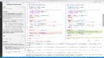
The section on assertions provides nice examples for how analog/digital assertions are constructed. Nothing mysterious here. For an ADC, the check quantizes the input voltage to an expected digital value and compares that value with the output of the ADC. For the DAC, simply invert this check, comparing the expected output voltage with the DAC output voltage.
UVM integration details will make more sense to UVM experts than to me (a UVM illiterate). I know it’s important and appears to be quite detailed in the examples.
The paper wraps up with a nice discussion on measuring linearity in these devices, a topic you wouldn’t find in logic verification, and a discussion on results of the analysis. My takeaway from the second point is that here is an opportunity to consider the randomization constraints set in the beginning. Overestimating these constraints could lead to more errors than observed in silicon, and, of course, underestimating could be disastrous. I expect getting this right probably requires some level of calibration against silicon devices.
Thought-provoking paper for me. You can read it HERE.
Also Read:
How to Update Your FPGA Devices with Questa
The RISC-V and Open-Source Functional Verification Challenge
Prioritize Short Isolation for Faster SoC Verification