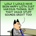
100X800 Banner (1)

Tensilica: We are #2 so we try harder

Tensilica: We are #2 so we try harder
by Paul McLellan on 06-20-2012 at 1:00 pm

The Linley group is the go-to source for information about the microprocessor market. If you go back to their roots in Michael Slater’s Microprocessor Report then they have been in the business for 25 years. We haven’t had microprocessors for that much longer. They just tagged Tensilica as being second in shipments of chips containing DSP cores. Last month Linley published numbers showing CEVA as #1 but, as I blogged about, they classified Tensilica and ARC as general purpose cores and didn’t include them in the DSP market. They have since reconsidered that position since, in fact, many Tensilica cores are used for audio, video and cellular (e.g. LTE) signal processing. For example, Tensilica is in the Audience chips in the iPhone. Linley now reckon that 1.5 billion chips were shipped in 2011 with licensable DSP cores and Tensilica is 20% of that market (so that would be about 300M DSP cores). Tensilica say that shipments of cores roughly doubled in 2011 from 2010.

Last year Tensilica announced that their licensees had cumulatively shipped over one billion Tensilica cores and they expect to pass two billion (cumulative) by the end of 2012. So roughly a billion Tensilica cores shipped during 2012, that’s impressive growth. Of course it is the nature of the IP business that you license a core and then…nothing happens. The chip has to be designed, prototyped, designed into a product, ramped to volume and only then do royalties flow (and you get on Linley’s radar).

As Mike Muller of ARM said to me years ago, “royalties always come later than you expect and are less than you expect.” When you are a big supplier, one reason is that some of your accounts will be big hits and some will not, but they all gave you optimistic predictions of the volumes they hoped to ship. For every iPhone that takes off like a rocket there is a Blackberry or a Lumia that isn’t selling because…well, everyone is buying iPhones. I remember in the early days of VLSI Technology when the PC business was taking off, we had about a dozen customers designing PC ASICs of one sort or another with a business strategy of being 25% of the PC market. We had no idea which ones would succeed but for sure not all of them. The answer pretty much turned out to be none of them.

Oh, and if you are visiting Tensilica they are about to move. But you are in the right place. They will be moving to the two storey building just across the street.

Totally off-topic, there is an interesting story behind the Avis tagline that I used as the title to this blog, as told in Robert Townsend’s book Further Up The Organization. Townsend went to his advertising agency DDB and asked the head how he could effectively get $2 of advertising for every $1 he spent, since Hertz was twice his size. He was told “just do this: promise that you you will not nitpick, that you will run whatever ad you select completely unchanged. you will have every person in this office moonlighting on your account.” After a couple of months DDB went back to Avis and told them that the best they had come up with was the “we’re #2 so we try harder” idea. Nobody seemed that keen on it but Townsend had promised to run the ads unchanged, so they did. The rest is history and it is now one of the most recognized taglines ever.


Atrenta Aquires NextOp

Atrenta Aquires NextOp
by Paul McLellan on 06-20-2012 at 10:00 am

Atrenta announced today that it is acquiring NextOp Software. NextOp sells a tool BugScope that provides assertion synthesis technology. This complements Atrenta’s SpyGlass products for improving the process for design of complex semiconductor IP and SoCs.

I went to Atrenta’s office to talk to Ajoy Bose (CEO) and Mike Gianfagna (VP marketing).

It’s not been a secret that Atrenta has been looking to do an acquisition, but one challenge being as large as they are is that it has to be a reasonable sized acquisition to make any difference. NextOp is a private company with no institutional investors. It is a couple of dozen people, half in San Jose (who will move into Atrenta’s building) and half in Shanghai (which will create a fifth R&D center for Atrenta, along with San Jose, India, Grenoble and, most recently, Sri Lanka where they have 20 people going to 30 by the end of the year).

Of course the other big aspect of an acquisition is that it should be synergistic with Atrenta’s existing business, not just be a bit of additional revenue. That is it should be more than additive and drive growth too. NextOp fits the bill. It is a good sized business with good momentum and the Atrenta channel should be able to start selling the product immediately into their 200-odd customers (NextOp has about a dozen customers including Altera, AMD, IDT, PLX and nVidia. They are mostly already Atrenta customers too).


NextOp seems to do for functional verification what Atrenta does for synthesis, static timing, place and route and so on. That is they don’t do any of those things but they make the whole process smoother and more effective, thus reducing cost, time-to-market and improving quality. NextOp looks at the results of simulations and generates assertions and functional coverage properties which can be used with simulation, emulation and formal verification to improve overall verification. They call this assertion synthesis.

NextOp will make a nice addition to IPKit too, which today encompasses a lot of factors like waivers that make flows based around integrating IP smoother. Now this can be expanded to include assertion and functional coverage properties, which was previously a hole in Atrenta’s offering.


Financial details of the transaction were not disclosed. Both companies are private and it took several months of negotiations to reach a deal (two companies with currency that nobody really has a good valuation for must make for some interesting discussions).

NextOp website. Atrenta website. Press release is here.


Shape-based IC Routing at DAC

Shape-based IC Routing at DAC
by Daniel Payne on 06-19-2012 at 8:05 pm

IC place and route is a big challenge so we see many EDA companies creating tools. On Tuesday at DAC I met with Dave Noble of Pulsic to get an update.

Notes

Dave Noble, VP Operations (EDA since 2003), Sperry Univac since 1974
– had been an EDA distributor for Pulsic as well

More leads qualified on Monday than all days of last year at DAC.

What’s new this year?
History
12 years old, technology from Zuken, a shape-based router with Japanese customers. Toshiba and Renesas steered the company to do analog routing. A tool to complement the skills of an IC layout designer, not replacing their job.
Take a 6 week manual route into one day, you still have to control the process. Automation or interactive routing, it’s your choice.

SHort learning curve by designs, easy to setup constraints, not a week long learning. Own GUI, not an integration into Cadence GUI. ROuting can be exported to OA.

Unity CUstom Digital Router – been around for 12 years now. Has STA built in to the tool flow, so you don’t have to exit the router to understanding timing impact.

Unity Analog Router – new this year. Not as automated as CiraNova, more intuitive to your existing analog flow. Constraints are annotated in the schematic. We distinquish between custom and analog IC layout. Analog centric routing. Online DRC by reading a Cadence deck.
– Could read a Calibre deck, but not there yet. TSMC has about 10 pages of rules for analog routing. Goal is DRC correct by design, also you can check and fix in a semi-automated fashion.

– Pyxis was a litho-aware router.

– Virtuoso : Custom router with some analog features.
– CiraNOva: Press the route button and hope for the best, but didn’t get what I wanted.

Unity Bus Planner – separate piece available.


CUstomers: Samsung, Micron, (DRAM, Flash, PCM). AMS companies in Japan and US, FPGA. Memory companies like the sophisticated shape-based approach for routing the IO. Network switching companies starting to use Pulsic routers.

Shape-based isn’t constrained to a grid, so results are more efficient with fewer jogs and vias. Not aimed at being an ASIC router company.

Reference flows at Foundry – most of our clients are IDMs so we aren’t qualified at TSMC and other foundries. Do have customers using 28nm at TSMC.

Development in the UK (Bristol, New Castle), Japan.

Privately held and funded. Growth plans – add analog routing. 2011 about 30% growth and 2012 about 25% growth. Hiring now.

Time based licenses, typically 3 years, including support and training.

Why you versus competitors? Manual routing is the primary competitor.

Evaluations: Used to be 9 months, now about 6 months. Set a criteria of success.

Any consulting services? Yes, we do some of that for our customers in terms of creating and optimizing a flow, working with their data.

3rd party: Cadence Connections, Mentor OPen Door, Synopsys inSync, SpringSoft.

12 months from now – continued revenue growth, more people (32 now), new products next year from internal development. Enough cash to last 3 years, so have conservative growth plans.

Japan – distributor is Jedat.

Release cycles – green build every 3 months, SCRUM methodology. Customers can track the progress of every bug filed, complete transparency.

Summary
Pulsic offers P&R tools for both digital and analog IC designers. They compete in a crowded market with: Cadence, Synposys (Magma), Mentor and A Toptech.


3D Thermal and Mechanical Stress for IC Packaging

3D Thermal and Mechanical Stress for IC Packaging
by Daniel Payne on 06-19-2012 at 8:02 pm

3D has been a growing buzz word in IC design and packaging for several years now, so it’s refreshing to actually find an EDA vendor that has developed tools to help analyze something like 3D thermal and mechanical stress at DAC. Continue reading “3D Thermal and Mechanical Stress for IC Packaging”


Executive Opinion: The Future of EDA is Bright

Executive Opinion: The Future of EDA is Bright
by pravin on 06-19-2012 at 7:30 pm

The days following a major conference like DAC are a good time to reflect on the overall health and vibrancy of the electronic design automation (EDA) industry. I’ve been in EDA for 21 years and built two successful startups, and over the last couple of years, have witnessed some decline in both new talent and in venture investment coming to EDA.


However, I am very optimistic that the future for EDA is brighter today than ever for a variety of reasons – the mobile computing revolution, a surge in semiconductor revenue, the transition to 20nm, and the emergence of 3D-IC manufacturing, just to name a few. These new industry trends and advanced process node challenges will likely make the EDA industry look more interesting to engineers, vendors, entrepreneurs, and investors.

Advanced process node challenges
The transition to smaller geometry nodes has enabled the semiconductor industry to create high performance systems-on-a-chip (SoC) with lots of functionality without compromising on overall power consumption. These versatile new SoC chips have helped spawn new market segments, the most successful being the smartphone and tablet markets. At 20nm, your mobile application processor will have a billion transistors, four processor cores, and processing power equivalent to what a typical desktop PC had just 3 years ago. It will have the ability to play full HD video with the graphics performance of a gaming console, while burning less power and providing longer battery life than ever before. 3D-IC manufacturing will enable stacking of ICs, resulting in packing even more functionality in a smaller footprint with overall lower power. The transition to smaller process nodes and the move to 3D-IC is accompanied by a myriad of technical challenges that should trigger the interest of the “problem solving” talent pool.

EDA is central to modern semiconductor advances
The revolution in semiconductor SoCs that is powering the mobile market would not have been possible without innovations in design automation software. 20nm brings a new variety of design challenges that stress every aspect of design automation. Billions of transistors and SoCs with multiple power domains mean new verification challenges. Simulation software has become more versatile over the past few years and has added new verification techniques like property checking and IP modeling, while continuing to speed up the core simulation. Newer emulation boxes are providing billion gate capacity for faster hardware bring-up and software debug for large SoCs. IC implementation offers new challenges in the areas of capacity, low power, and multi mode, multi-corner timing closure of gigahertz chips. 20nm is bringing new manufacturing requirements like double patterning that need to be handled effectively during design implementation.

EDA Upsides
To thrive in the EDA industry, engineers need a unique skill set that blends both electronics engineering and computer science. Specialization in design knowledge along with algorithm and software expertise creates a strong, sustainable, and marketable skill set. There are over 70 niches in the EDA market, giving opportunities to engineers to explore and contribute in many new areas. EDA is one of the very few industries that remain stable during recessions and downturns, as customers always continue to invest in new design starts, thereby guaranteeing predictable and long term employment.

On the vendor front, EDA companies have been able to build a strong business around their anchor products. The move from perpetual to term licenses has resulted in a much more predictable revenue model for EDA vendors. Innovative products and increasing design challenges have also resulted in improved pricing and better revenue for all EDA companies, large and small.
EDA is a great industry for entrepreneurs, and I can vouch for that from my personal experiences. Every transition to a smaller process node brings new disruptions to the design flow, opening new doors for entrepreneurs to challenge the incumbents. EDA is perhaps the only industry where a leading edge, multi-billion dollar company is willing to use software from a startup company on its next generation design. At this year’s DAC there were more than ten new startups exhibiting. From an investor perspective, the cost of building an EDA startup is relatively small compared to most industries, and many EDA startups have gotten to first revenue with less than 10 engineers. Since EDA startups can reach profitability fairly quickly, investment in EDA can result in superior returns if managed carefully. In the last three years, EDA startups have had over $800 million in exits resulting in great returns for investors.

Conclusion
The EDA Consortium, a representing body of the EDA industry, has a slogan “EDA: Where Electronics Begins.” It sums up the importance of this industry and how it affects the $300 billion semiconductor market. EDA technical challenges are more dynamic now than ever, and will continue to be a hotbed of engineering innovation, a driver of semiconductor advances, and a vibrant business.

Pravin Madhani is theGeneral Manager, Place and Route Division, at Mentor Graphics.


It takes an act of Congress…

It takes an act of Congress…
by Beth Martin on 06-19-2012 at 4:29 pm

Foreign students earn roughly two-thirds of the total engineering Ph.D.s earned in the U.S., yet there is no policy to allow, let alone encourage, them to stay in the U.S. after graduation. I was aware of this problem 14 years ago when I started working in EDA, but haven’t paid much attention since then.

So, I scoured the congressional websites to learn what our leaders have been up to in terms of making it easier for foreign engineers to work and create jobs in the U.S.. I also stumbled on a couple of bills that promote and foster science and technology innovation. I found less than I expected, many already dead or stalled. There are imponderable feats of politics involved in getting anything to the president’s desk for signing, but here are the main bills you should know about:

The Innovate America Act 2011 (S.239) was introduced in January 2011 by Senator Amy Klobuchar (D-MN) with bi-partisan cosponsors. It would expand research tax credits, tax credits for donating equipment to schools, fund 100 new STEM high schools, and remove regulatory barriers for exporting industries. It was referred to the Committee on Finance, of which Klobuchar is a member, and there it died.

But, a similar bill, the America Innovates Act of 2012 (H.R.4720), introduced by Rush Holt (D-NJ), would establish an Innovation Bank to fund science and technology job training. There has been no action on this bill yet.

There’s been more action specifically around immigration reform, with equally little to show for it. Zoe Lofgren (D-CA) and 25 cosponsors introduced the Immigration Driving Entrepreneurship in America (IDEA) Act of 2011 (H.R.2161) in June 2011. This would have given priority worker visas for immigrants with master’s degree or higher in science, technology, engineering, or mathematics (STEM workers). I say “would have” because the IDEA Act was sent to some committee to die.

But wait! The Fairness for High Skilled Immigrants Act(HR 3012) was introduced by Jason Chaffetz (R-UT) in November 2011 and passed the US House with a stunning 89% aye votes, even though the bill doesn’t have a catchy acronym. However, it’s been blocked in the senate by Charles Grassley (R-IA). I think there are ways to get around the hold (through a cloture motion), but what do I know? Stay tuned.

Then there is the Startup Act 2.0(S. 3217) introduced by Senator Jerry Moran (R-KS) in May 2012, and hearings should happen soon. This bill reforms immigration law to create new STEM visas, creates an entrepreneur’s visa, and eliminates per-country cap for work visas. You can read a thoughtful opinions on it at TechCrunch. There is a fair amount of press on this one, from the Washington Post to the Huffington Post.

Also introduced in May was the SMART Jobs Act(S. 3192) from Senator Lamar Alexander (R-TN). The Sustaining our Most Advanced Researchers and Technology Act (really? All that just to get the SMART acronym?) is designed to keep foreign-born US grad students here to work. A neat part is that green cards issued under this visa rule wouldn’t count towards the existing per-country caps. It’s getting a lot of support from technology companies and organizations, so maybe it will get some traction.

If the SMART Jobs Actfails, there’s always the similar STAR Act of 2012(ready for this? STAR=Securing the Talent America Requires for the 21st Century Act of 2012[S. 3185].Seriously, I imagine some high-fives going around the marbled halls for that one.) This one was introduced by Senator John Cornyn (R-TX), and would provide additional green cards for skilled immigrants in STEM fields.

Considering that only about 4% of introduced bills ever get past the committee stage (based on 2009-2010 data), there’s little hope any of these bills will become law. The best chance to exercise your influence (aside from handing over a chunk of your wealth) is to call or email your senator and representative and urge them to act on these bills. You can find your senator and representative through this webiste.

M. Beth


Selecting Non Volatile Memory IP: dynamic programming from Novocell Semiconductor lead to a lower “Cost Of Ownership”

Selecting Non Volatile Memory IP: dynamic programming from Novocell Semiconductor lead to a lower “Cost Of Ownership”
by Eric Esteve on 06-19-2012 at 9:07 am

NVM IP offering from NovocellSemiconductor is based on SmartBit, an antifuse, One Time Programmable (OTP) technology, and the OTP block are embedded in standard Logic CMOS without any additional process or post process steps and can be programmed at the wafer level, in package, or in the field, as end user requires. What makes SmartBit technology unique is the “breakdown detector”, allowing to precisely determining when the voltage applied to the gate (allowing programming thememory cell by breaking the oxide and consequently allowing the current to flowthrough this oxide) will effectively have created an irreversible oxide breakdown, the “hard breakdown”, by opposition of a “soft breakdown” which is an apparent, reversible oxide breakdown. This is a first advantage: when the OTP programming step is completed, the user can be sure that every bit will have been set at the forecasted value. Apparently, this is not the case with each of the various OTP architectures, even if this is what you would naively expect from any NVM technology!

How do Novocell competitors proceed to program an OTP block, without this “breakdown detector” feature? They have to determine the“optimal programming timing” (the set time) provided to program each bit, which is determined for each specific foundry process (by technology node, and variation) and program the block according with this “set time”. Unfortunately, this ‘set time’ programming method will always result in some bits being ‘remnant’ bits un-programmed in the initial programming cycle. To be sure that every bit in the NVM block will have been set to the correct value, an additional programming cycle –at least- will be necessary to increase the yield. This approach is obviously time consuming (it takes at least twice the initial programming time), which can be pretty costly if, for example, you have to program the OTP using the tester, at wafer or packaged IC test step, when you consider the cost related to the test time on multi-million dollar devices. Another good point for SmartBit architecture: not only the programmingis more reliable, deterministic, but the cost of ownership linked to theprogramming step is cheaper.

Novocell competitors are trying to offer a safer approach, based on Error Correction circuitry or redundancy. Just take a look at what this precisely means, if we consider that some IP includes a full 2X redundancy of bits in order to achieve yield and performance requirements. Full redundancy can lead toeffectively doubling the area required on the chip for the customer-ordered bit density! A safer approach, even if it is theoretically not as safe as SmartBit, at the price of Silicon over cost. This over cost can be highly penalizing, when the NVM block is large and the device in production generating volumes that we see in the Consumer Electronic or Wireless Handset segments: million if not dozen of million units! Again, a costly tradeoff for an inferior programming methodology versus the Novocell dynamic approach based on “breakdown detection”…


Clearly, one of the Novocell’s differentiator is reliability, thanks to the “breakdown detector”. We also have seen that choosing SmartBit technology can dramatically reduce the total cost of ownership, by reducing programming time by a factor of 2 or more, and by using to a smaller NVM IP block size, leading to a smaller real estate or chip size than competitors, being forced to add redundancy to reach the same level of reliability – or yield.

Eric Estevefrom IPNEST –


What’s new with HSPICE at DAC?

What’s new with HSPICE at DAC?
by Daniel Payne on 06-18-2012 at 5:50 pm

One year ago I met with Hany Elhak of Synopsys to get an update on what was new with HSPICE in 2011, so this year at DAC Hany met me at the Synopsys booth for a quick update.

HSPICE has something called Precision Parallel so with 16 cores your IC circuit simulations will have about 10 x speed up compared to a single core.
Continue reading “What’s new with HSPICE at DAC?”


TSMC Threater Presentation: Solido Design Automation!

TSMC Threater Presentation: Solido Design Automation!
by Daniel Nenni on 06-17-2012 at 9:00 pm

For a small company, Solido has some very large customers and partners, TSMC being on of them. Why? Because of the high yield and memory performance demand on leading edge technologies, that’s why.

Much has been made of and will continue to be said on the march of Moore’s Law. While economics of scale and performance vs. power are the main justifications, there are increased design challenges that make designs of prior decades seem quaint by comparison. Smaller transistors allow for lower cost per function and more power efficiency, but they also come with increased variation effects, making performance vs. power vs. yield tradeoffs a necessary part of the design flow.

With each successive process shrink, there is a corresponding increase in the number of SPICE simulations required to push design performance while ensuring manufacturability. Solido Design Automation provides solutions for reducing the number of simulations needed during design and verification, while still providing the same or more visibility into design choices, impacts on yield and risk. As a leading provider of efficient variation analysis tools, Solido continues to collaborate with TSMC to deliver effective analysis capabilities on the latest nanometer technologies, supporting designers of memory, standard cell, low power, and analog/RF circuits.

Memory designers have perhaps the greatest challenge in maximizing their design performance within the capabilities of a particular process technology, needing to validate yield and performance to 4-6 sigma on bit cells and sense amps and 2-4 sigma at the array level. While Monte Carlo is the preferred solution, it’s simply impractical to simulate the billions of points needed for 6-sigma analysis. Since the analysis still has to be done, a number of approaches have evolved that seek to bypass Monte Carlo, but they each suffer limitations in accuracy, scalability and, especially, verifiability.

Solido’s Memory+ Suite goes back to the core Monte Carlo analysis designers trust and handles the billions of samples with intelligent adaptive techniques to focus simulation resources towards the high-sigma tails of the distribution. Since Memory+ uses actual Monte Carlo samples, it is able to provide simulation results around the target sigma, high-sigma corners for use in design development and even the full PDF. These options give designers the detailed insights they need into non-linear effects, design sensitivities to make informed sizing decisions.

Unlike other approaches, Solido’s Memory+ is able to handle the more severe non-linear responses, rendering it applicable to a broad range of memory cells. In the following example, a 3- or 4-sigma analysis would appear linear with extrapolation completely missing the failure regions occurring at +/- 4.5-sigma.

Additionally, with the full PDF available for both the bit cell and sense amp, Memory+ can provide 3-sigma analysis at the system level, allowing designers to explore performance vs. yield tradeoffs directly. The following table shows the results of a 3-sigma analysis on a 256Mb SRAM array using the Memory+ System Memory tool, enabling visibility into the tradeoff between timing and system-level yield, in a matter of minutes. The tool is also applicable to system-level DRAM analysis.

Using memory design as just one example, Solido is able to provide designers with the necessary tools to analyze yield and performance, faster and with more consistent quality than before. As shown with Memory+, memory designers can quickly analyze designs at the cell level to 6-sigma and the system-level to 3-sigma, while keeping Monte Carlo and SPICE level accuracy.