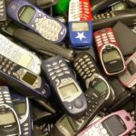
Synopsys IP Designs Edge AI 800x100

Customers Talk About Reliability, Low-Power and 3D

Customers Talk About Reliability, Low-Power and 3D
by Paul McLellan on 05-09-2012 at 1:13 pm

At DAC in San Francisco this year, Apache once again have a mixture of presentations by customers on their use of Apache tools and presentations by Apache themselves on their products. Most of the customer presentations are given just once, but the product presentations are given multiple times over the three days.

I think one of the hot topics at DAC this year will be 3D-ICs (TSVs etc). One on of the first places that 3D chips are being used is building stacks of memory die, so the Samsung experience looks especially interesting.

Here is a list of all the customer presentations. The product presentations are interspersed between the customer presentations.

  • Samsung-DRAM: System-level Power Noise Analysis and Optimization with Measurement Correlation Results for Multiple DRAMs with TSV
  • UC San Diego: Considerations for Designing and Simulating Memory Interfaces for 3D/Stacked-die Designs
  • Renasas: Enabling Accurate and Efficient RTL Power Analysis and Optimization Methodology for Low Power Designs
  • LSI: Power Noise and Other Simulation Considerations for Energy-efficient SoCs
  • Samsung-SSI: A Chip-Package Simulation Methodology for Ultra-Large Low-Power Mobile ICs
  • Ciena: Power Noise Analysis with Silicon Correlation Results for Complex 32nm ASIC Designs
  • NXP: Full-chip Substrate Noise Coupling Analysis and Noise Isolation Structure Design Experiments
  • Aptina: Evaluating Design Options and Trade-offs through Full-chip Substrate and Metal Layer Noise Analysis for a Commercial Image Sensor Chip
  • AMD: Electrostatic Discharge (ESD) Simulation and Sign-off Considerations for Complex GPU and APU Designs
  • nVidia: A Dynamic Simulation Methodology for Diagnosis and Predictive Simulation of HBM/CDM Events
  • ST-Ericsson: Simultaneous SI and PI Analysis for High-speed IO Designs for Mobile Applications

Full details, including the presentations times and a short summary of each presentation are here. If you are interested, then you can register to attend on the same page.

One other event is at the pavilion panel (booth 310) at 10.30 on Monday where Aveek Sarkar of Apache is one of the panelists on a panel called Power to the People, along with Clive Bittlestone of TI and Robert Patti of Terrazon Semiconductor.


Sagantec Update: More EDA Consolidation!

Sagantec Update: More EDA Consolidation!
by Daniel Nenni on 05-08-2012 at 7:00 pm

Adding sophisticated 2D dynamic compaction technology to address 20nm and 14nm challenges. Santa Clara, California – May 3 ,2012 – Sagantec today announced that it has acquired Dutch startup NP-Komplete Technologies BV (Eindhoven, The Netherlands) for its physical design compaction and migration solutions based on a sophisticated 2D dynamic compaction technology. NP-Komplete Technologies (NPKT) is a provider of innovative DFM solutions, and physical design optimization engines. Terms of the acquisition are confidential.

Having worked with Sagantec over the years, I can tell you a little more of what is going on here. Sagantec has been leading the process migration march since ~1996. That was some 16 years and 10 semiconductor process nodes ago. During that time Sagantec introduced the industry’s first hierarchical compaction/migration tool, they added Cadence Virtuoso, OpenAccess, and Pcell support, they added analog design constraints, etc… Sagantec actually coined the term “process migration” and made it a viable EDA market segment.

The Sagantec engineering team in the Netherlands is now fully integrated with the NPKT team with the combined team working together on enhancing the tools and addressing future technology challenges.Following the acquisition, NPKT is now a wholly-owned subsidiary of Sagantec and continues to develop and provide advanced layout compaction and DFM solutions.

The Eindhoven guys wrote the original Sagantec compactor then re-wrote it for Takumi’s DFM products and later spun out to re-write it again for NKP. This perpetual march down the shrinking geometry path has epitomized our industry since Moore “enacted” his law (observation) in 1965, and this trend is not going to go away anytime soon. However, as dimensions shrink further and deeper, each new technology transition seems to be a little more disruptive than the previous ones, presenting new concepts and more difficult challenges for design rule compliance and layout migration. The current 28nm design rules and evolving 20nm technologies are really complex and hard to manage, so adding some innovation and refreshing the compaction engine will help to solve the 20nm puzzles.

The NPKT migration technology is an automated layout optimization technology, and was designed from the ground up to address the latest challenges of 20nm design rules. Since most of the new rules are enforced to overcome manufacturability-related challenges that impact yield, it takes a sophisticated 2D compaction technology to make necessary modifications to create a DRC clean layout. The NPKT technology has already been proven with DRC clean results at several tier-1 semiconductor companies, and used on multiple 28nm and 20nm technologies of leading-edge foundries. The addition of this new technology and expertise enables Sagantec to better address the new challenges and overcome technology discontinuities that result from the introduction of new layers and new types of design rules associated with the 20nm process node while producing best possible quality results.

Sagantec will have this and other innovative technologies at the Design Automation Conference in San Francisco next month. Even more importantly, Sagantec will have me in their booth talking about the challenges of 20nm and how the fabless semiconductor ecosystem will continue to thrive in the coming process nodes. See you there!


San Francisco Bars

San Francisco Bars
by Paul McLellan on 05-08-2012 at 6:00 pm

If you are visiting DAC and want a drink in the evening then you are in an interesting city and you don’t have to go to a bar just like the ones in the city where you live. Here are a few unique places but take note, most of these places don’t serve any food, they are all about the drinks:

Bourbon and Branch. It is an old speakeasy. You have to make a reservation on their website and they will tell you where the bar is and what the password is. You then have to ring the bell at an unmarked door and give the password. OK, a bit hokey, but they have incredible cocktails. In fact, the real old speakeasy with secret exit tunnels is downstairs (they might take you on a tour if you ask). It’s actually on the corner of O’Farrell and Jones. There’s a bar next door called the Library where you don’t need a reservation (and you can exit through it via a secret bookcase from B&B itself). No food.

Smugglers Cove. 650 Gough Street. Over 300 rums and the best rum cocktails around in a fantastic tiki-type atmosphere. Make sure you take the address, they don’t really have a sign outside and it is just a regular store-front, so it is hard to find the first time. Look for a red and a green navigation light. #19 on Drinks International 50 best bars in the world 2011. TheJet Pilot is my favorite drink. No food but there are lots of places if you walk down the hill. Open until 2am.

Tommy’s. 5929 Geary (near 23[SUP]rd[/SUP] Avenue, so yes, a long way from downtown on the 38 bus). OK, if rum is not your thing but tequila is then you’ll love Tommy’s. A carefully chosen selection of tequila. The tequila menu is here. Ignore the restaurant and head for the bar. Julio (Tommy’s son) will give you a tequila education. They were the first bar to switch to 100% agave Tequila…35 years ago. They have some Cuervo Gold but won’t sell it to you, they just have it for educational reasons to show you why you shouldn’t drink it! #30 on Drinks International 50 best bars in the world 2011. They also make the classic Tommy’s margarita. Mexican food. Closes on Tuesdays and at 11pm on other days.

Toronado. 547 Haight Street. Beer lover’s paradise with about 60 beers on tap including many rare ones. The up-to-date list is here. They have some seats but you probably won’t get one. Cash only, but you won’t need much, the prices are low. No food, but you can order sausages in the store next door and they’ll bang on the wall when they are ready, or lots of other choices on Haight Street. Open until 2am.

Black Horse London Pub. 1514 Union Street. The opposite of Toronado, no draft beer at all. Microbrews served out of a tub of ice. The smallest bar west of the Mississippi apparently. Only fits about a dozen people. Go early or you will be lucky to get in. It’s cosy but everyone is really friendly when I’ve been there. No food, obviously (no room for a kitchen) but lots further along Union Street. Open until midnight.

Zeitgeist. Corner of Duboce and Valencia. About 50 different beers on tap. Huge beer garden out the back where there are lots of people smoking. And I don’t mean cigarettes. Many cyclists and bike messengers go here, they have a huge bike-rack in the beer garden. They have really good hamburgers and sausages and sometimes the Tamale Lady is around. Cash only. Open until 2am. They get incredibly busy on sunny weekend afternoons.

Also see the bars near Moscone (after the restaurants).


Is PHY IP really strategic? Just take a look at the various legal offensives running these days…

Is PHY IP really strategic? Just take a look at the various legal offensives running these days…
by Eric Esteve on 05-07-2012 at 12:02 pm

Last week, at the same time I was writing a blog about PHY IP market, claiming that this market was shaken, several events happened – not on the pure business side, but on the legal side. This means that I will have to carefully check before using each word of this blog!

If you remember, the blog conclusion was focusing on V Semiconductor, a start-up created in 2008, founded by former Snowbush’ employees, who decided to leave the company short after acquisition by Gennum. In the meantime, V Semi has launched a revolutionary SerDes, revolutionary because it is based on a digital PLL and not on oscillator PLL or even on LC tank PLL, and the technology has been implemented on Intel 28nm technology to support multi-standard protocol PHY, to be used by FPGA start-up, and probably acquired by customers developing 10G Ethernet PHY. This technology looks so attractive that V Semi was about to be acquired; by which company? Considering the on-going legal battle, I am sure you will forgive me to stay quiet about this… and call it “Company A”. But, if you want to know more about the, now previously, expected buyer, you can go on Law360 website, and try to figure out which company it could be. So we are now at late 2011, V Semi founders are finalizing the discussions with “Company A”, a letter of intent is written for an acquisition to be closed on February the 14[SUP]th[/SUP] of 2012. At the same time, Semtech, a fabless company, is also finalizing the discussion with Gennum, in order to acquire the company…

So far, these were usual moves happening in the Semiconductor and design IP industry, merger and acquisition (M&A) are pretty frequent on this fast moving market. The surprise comes when Gennum decides to sue V Semi, filling a Canadian lawsuit on February 3, 2012, against V Semi. As we did not have a chance to read this lawsuit, we prefer not to comment it! But the immediate result is that the company being engaged in the process of buying V Semi has decided to pull its offer.

It seems that the legal battle field can also be an extension of the more classical competition, where companies are fighting for market share by using marketing and sales forces. Can we say that this Semtech vs V Semi case is such an example? It’s probably too early to know the reality behind this legal battle. Nevertheless, V Semi management has reacted like if the initial (legal) attack from Semtech was just a way to keep away the industry of using V Semi revolutionary SerDes, as they have, on April 26 filled a $150 million lawsuitagainst Semtech, the former Gennum CEO, as well as a person who was in charge of due diligence about V Semi, when working for another company (Company B in V Semi case) when this “Company B” was thinking about buying V Semi technology!

I remember when I was far younger, watching “Dallas” serial at TV. Looking at what is happening today in the SC and IP industry make you feel that Dallas is a fairy tale for five years old kids, when comparing!

That’s all for today…but I will stay tuned, as I guess that this is not the end of the PHY IP real saga!

By Eric Esteve from IPnest


Achieving Rapid Verification Convergence of ARM® AMBA® 4 ACE™ Designs using Discovery™ Verification IP

Achieving Rapid Verification Convergence of ARM® AMBA® 4 ACE™ Designs using Discovery™ Verification IP
by Eric Esteve on 05-07-2012 at 3:17 am

Synopsys is consolidating the company positioning on Verification IP. We have announced the launch of Discovery VIP in Semiwiki, in February this year, and we have commented about the acquisition of nSys and ExpertIO in January. This webinar, “Achieving Rapid Verification Convergence of ARM® AMBA® 4 ACE™ Designs using Discovery™ Verification IP”, to be held on May, 8 at 10am PDT, will allow the audience to better understand Cache coherency management problematic. Traditionally, cache coherency management has largely been performed in software, adding to software complexity and development time. With AMBA 4 ACE, system level coherency is performed in hardware, providing better performance and power efficiency for complex SoC designs. However, this shifts much of the complexity of verify cache coherency to functional verification.

This webinar begins with a short overview of the challenges of verifying a coherent design and goes on to show how the features and architecture of Synopsys’ new Discovery Verification IP helps overcome these challenges to simplify the verification of ACE designs.

The ever growing design time spent in verification, we have recently read figures of 70% of the overall hardware design effort being associated with the verification, is creating a demand for most efficient EDA tools, and accurate Verification IP (dedicated to a specific protocol).

The next picture is useful to understand the cost breakdown associated with Verification. If you look at the middle left box, you see a 3X cost (or license count, or resources) increase for almost every task (except “Tool, Support and Service” with 20% only). So, offering a 3 to 6X run time improvement is welcome, to keep the design schedule and consequently the time to market within reasonable limits.

You can log to this webinar here

From Eric Esteve from IPnest


TSMC 20nm Challenges!

TSMC 20nm Challenges!
by Daniel Nenni on 05-06-2012 at 7:00 pm

Now that the 28nm challenges are dead
It is time to look ahead
The tabloid pundits may not agree
But Moore’s law again you will see
The semiconductor ecosystem is humming
(2X gate density -20%+ performance-20%+ power savings)
The 20nm design starts are coming!

Okay, I’m really bad at poetry. Gambling however, I do pretty well. Las Vegas is my favorite destination, a mere 6 hour Porsche drive from Danville. It’s not just the math of gambling that’s intriguing, it’s also how you read a person, a play, or situation. I literally won all of my bets on 28nm and 20nm looks like another great gambling opportunity. I have two more kids to get through college so put your money where your mouth is.

Here is why the 20nm challenges will be vanquished in record time: GREED, simple as that! As I mentioned before, the semiconductor ecosystem consists of a very large crowd of very smart people with very big egos who really like making money (me for example). Whomever solves the 20nm design and manufacturing puzzles first not only gets fame, they also get fortune. Talk about motivation. And who doesn’t like solving puzzles?

20nm blogs-white papers-webinars are in play
20nm test chips arriving every day
40nm we learned how to yield
28nm we yearned for capacity
20nm will be an even bigger payday
!

Better? Intel has done us all a really big favor. They are shooting their mouth off, motivating the masses, because who in their right mind would NOT want to prove Intel wrong? Especially if you can make money while doing it. Sign me up!

Here is the biggest bet: What will the TSMC 20nm ramp look like?

Remember, even though the tabloid press had 28nm “not yielding at all” and “shut down for weeks” in Q1 2012, the ramp thus far has beat expectations. The questions are:

[LIST=1]

  • Will 20nm be on par with 28nm?
  • When will the 20nm ramp officially start?
  • How far behind the Intel 22nm SoC mobile version will it be?


    According to the SemiWiki crowd, Apple will be at TSMC 20nm:

    Who will Apple partner with at 20nm?

    [LIST=1]

  • TSMC 38.04%
  • Intel 25.00%
  • Neither (stay at Samsung) 19.57%
  • Both 17.39%

    So you might want to factor that extra motivation into your gambling equation.

    My trip this week was off a bit due to the national Taiwan holiday on Tuesday so here I sit in the EVA Executive Lounge on a sunny Saturday afternoon.

    Don’t feel bad for me there’s an open bar
    Don’t feel bad for me I have a beautiful car
    Don’t feel bad for me this week I’m fishing afar


  • Formal Verification, there’s an App for that

    Formal Verification, there’s an App for that
    by Paul McLellan on 05-06-2012 at 6:00 pm

    The success of Apple’s AppStore has made people aware that software doesn’t have to be delivered in a big monolithic lump. Indeed, going back a bit earlier, Apple’s iTunes store made people aware that you didn’t have to buy a whole album if you only wanted a track or two.

    EDA applications in today’s server-farm world suffer from another problem: you might want to buy a lot of one capability of a tool, because you use it a lot, and a little (or none) of another capability that you rarely make use of. The monolithic approach lacks this flexibility.

    Jasper’s flagship JasperGold product has historically been delivered in a form that included all the capabilities, and at a price point that reflects that breadth. In some ways this works well for formal verification since different proof engines can work together: if you can’t prove something with engine A then maybe engine B can prove it. It only takes one engine to succeed. It’s a bit like solving differential equations. You just have to find some way to come up with an answer that differentiates back to the equation you started with, and it is hard to predict which approach might work.

    JasperGold is being restructured into a sort of backplane consisting of a common database and a common user-interface. Into this backplane you can plug one or more Apps.

    The initial Apps that are available are:

    • Formal Property Verification (FPV) App
    • Connectivity Verification App
    • X-propagation Verification App
    • RTL Development App
    • Architectural Modeling App
    • Control/Status Register (CSR) Verification App


    In the future additional Apps will be added. There are still a few products (Active Prop Property Synthesis, Post-Silicon Debug and the Intelligent Proof kits) which are still delivered as separate line-items outside of the App infrastructure.

    This App approach to delivering capability fits much better with the realities of how design is done today. Very large design teams, large server farms providing compute resource, internationally distributed development.

    This App approach (Approach?) makes it straightforward to run multiple applications on the same block, sharing the work product through the common database, and so reducing the total effort for the project. It is easy for a user to run multiple applications on the same block and launch parallel applications through the same user interface. Parallel jobs can be launched through the common interface with the results from all the parallel jobs being collected back into the common database. Overall, it allows for more flexible deployment of software licenses, and thus capabilities, than the monolithic approach.

    More details of JasperGold Apps are here.


    Where to eat lunch or get a beer at DAC

    Where to eat lunch or get a beer at DAC
    by Paul McLellan on 05-04-2012 at 11:17 pm

    You are going to DAC. And you don’t want to eat a Moscone Center rubber chicken Caesar salad for lunch. But you lack local knowledge. So here are some places within a 10 minute walk. These are just places I like. Nobody is paying me to recommend them.

    Places to eat
    The food court in the San Francisco Center on Market Street between 4th and 5th Street. This is to normal mall foodcourts the same way San Francisco Airport food is to normal airports. It’s actually good. There are two food courts, but far and away the best is the one at the 4th street end of the building. Go in the first entrance you come to walking along Market Street and go down the escalator. It has an amazing selection of ethnic food (Vietnamese, Korean, Thai, Japanese, Mexican, gourmet burgers, even Vegan Chinese…). There is another level with more expensive restaurants on the 4th floor (mostly not open for lunch). I like the Straits Cafe (Singaporean food) which does do lunch too.

    Indian: Chaat Cafe on the corner of 3rd Street and Folsom. The Tandoori mixed grill is a particularly good bargain if you have a crowd.

    Thai: Osha on another corner of 3rd Street and Folsom

    Mexican: Chevy’s on corner of 3rd Street and Howard Street

    Brew pub and tapas (yes, both): Thirsty Bear on Howard between 3rd and 2nd Streets

    Pizza: California Pizza Kitchen on 3rd between Mission and Market Streets

    Chinese: Henry’s Hunan on Natoma Street just off New Montgomery Street. Don’t miss Diana’s Special Meat Pie.

    Hawaiian: Roy’s on Mission between 2nd and 1st (pricey, take a salesperson to pay the bill!)

    Japanese: Ame in the St Regis Hotel on the corner of Mission and 3rd Street. Fabulous. Not open for lunch. But take a C-level executive to pay the bill.

    SFMOMA (see below)

    Bars
    The Pied Piper Bar in the Palace Hotel on the corner of Market Street and New Montgomery Street. Old fashioned bar with an amazing huge painting by Maxfield Parrish. My favorite bar in the area.

    The Upstairs bar in the W hotel on the corner of 3rd and Howard Streets (not the one on the first floor). Maybe too trendy…

    House of Shields on New Montgomery Street between Mission and Market. Live music for over 100 years, since the earthquake (the 1906 one).

    Top floor bar in the Marriott Hotel on the corner of 4th and Mission. Great place to view the whole city and watch the sunset. Find the right elevator and go to the 39th floor.

    The best wine bar in San Francisco is District on Townsend between 3rd and 4th. And the best brewpub is 21st Amendment on 2nd Street between Bryant and Brannan. Both are a little outside the 10 minute range, more like 15, and both have good food too.

    Place to spend a spare hour or two
    San Francisco Museum of Modern Art (SFMOMA) on 3rd Street between Howard and Mission. Closed on Wednesday. The food in the cafe is good too.

    Comment
    If you live in the city or know it well, then feel free to add your own recommendations in the comments.

    Map
    Everywhere is on this map (except District and 21st Amendment). That’s how close they are. You don’t have to have a crummy hamburger in one of the best foodie cities in the world.


    GlobalFoundries 2012 Update!

    GlobalFoundries 2012 Update!
    by Daniel Nenni on 05-04-2012 at 8:55 pm

    What’s new with Glofo? Quite a bit actually. It was interesting to see a Made in America: Global Companies Expand in U.S. Towns segment on semiconductors! Give it a look, I enjoyed it. It’s an election year, jobs are key to any election, so it did not surprise me to see President Obama making the rounds:
    Continue reading “GlobalFoundries 2012 Update!”


    It is free after you pay for it and there is a one-time annual fee: The Case for FD-SOI

    It is free after you pay for it and there is a one-time annual fee: The Case for FD-SOI
    by Camille Kokozaki on 05-04-2012 at 7:09 am

    In one of Portlandia’s TV program sketches, there is a funny interchange between a carrier salesperson and Fred Armisen (of SNL fame) who was trying to buy a phone. One chuckle line was a statement by the seller that the phone was free after paying for it and that there was a one-time annual fee. With this anecdote as a mental backdrop, the question for making the case for a new technology is: Is there a free gain? How much effort is really needed? The technology topic here is FD-SOI. This SOI exposé attempts to highlight the merits of FD-SOI (fully depleted Silicon-On-Insulator, and/or UTB-SOI, defined further below) which is now being looked as a viable technology offering since bulk CMOS is showing limits with technology node scaling. SOI technology is certainly not new in terms of having attractive leakage characteristics when compared to bulk C-MOS. The SOI consortium has announced a joint collaboration by ARM, Global Foundries, IBM, STMicroelectronics, Soitec, CEA- Leti to promote the FD-SOI technology and its value in mobile communication applications. The benefits are stated to be that Power/Performance metrics are excellent specially at lower voltages, simpler manufacturing and lower leakage.

    Joël Hartmann (Corp VP or front-end manufacturing and process R&D at STMicroelectronics) made a compelling case for FD-SOI at the latest GSA Silicon Summit in April and he highlighted that this technology is a main contender now that the bulk C-MOS is reaching its feature size limits (beyond 20nm that is) where short channel effects make bulk unworkable. ST is counting on FD-SOI at least for its 28nm and 20nm road map and will have products this year using 28nm FD-SOI. The industry’s alternative choice for advanced nodes is FinFET and was discussed earlier by Paul McLellan. Beyond bulk, fully depleted devices will be needed for improved electrostatic control. FD-SOI can be further turbo-charged by adding ultra thin box back body bias (UTB-SOI) with added performance specially at lower voltages. In the same event, Dr Chenming Hu succinctly outlined the main differences between FinFET and UTB-SOI in that for FinFET the body thickness has to be less than the gate length Lg with larger Ion current and foundry investments, whereas the UTB-SOI requires thickness less than 1/3 the gate length, with a good back-bias option and SOI supplier investments. The arguments in favor of FD-SOI as stated by STMicroelectronics are:

      [*=1]the use of the same Back-end process,
      [*=1]only 20% of FD-Specific Front end process needs new development,
      [*=1]wafer costs (process and substrate) are similar,
      [*=1]10% better lead-time is achievable,
      [*=1]no added Capex are needed since the same equipment is used,
      [*=1]the process is portable through shrink and scalable to 14nm.

    In the future FinFETs can also be built on top of SOI. The STMicro charts below illustrate how much power and performance can be gained using the UTB-SOI technology. At 1.0V 28nm FD-SOI with back bias can achieve a 94% performance boost over 28LP and at 0.6V a remarkable 730% improvement can be seen. More impressively at low Vdd the energy efficiency in (DMIPS/mW) literally goes through the roof as evidenced in the upward tilt of the top left curve. These are compelling numbers that merit notice and explain the road map direction of STMicroelectronics.

    It does thus appear, in an interesting way that performance and energy efficiency gains can be free after developments paid for them and that there is a one-time development fee that needs to stay annual to keep the bits pumping in the ever shrinking geometries. Now you also know that I will stretch words to fit my anecdote in the hope that you realize I am just word playing here to get you to read, to be informed and freely entertained.

    References:
    GSA Silicon Summit April 26, 2012 Mountain View, CA (The source for most of the graphics and data)
    SOI technology for the GHz era – by G. G. Shahidi
    Evaluation of a fully-depleted SOI for next generation Mobile Chips – by Horacio Mendez Executive Director, SOI Industry Consortium