I went to Warren East’s keynote speech at ARM Techcon today. There had been some hints earlier in the week that some significant announcements would be made and, while they were not earth-shattering, I think that they will be significant in the long term.
One interesting thing that Warren pointed out is that the ARM partner alliance is over 1000 companies strong. I don’t think anyone else can come anywhere close to that. It covers semiconductor partners, EDA partners, system companies, embedded software companies, standards bodies and more. It is quite an achievement to build up that large a portfolio of support so quickly. Back in the mid-1990s when I was at VLSI Technology, ARM had to set up a fund (that VLSI contributed to) to pay the real-time-operating-system companies such as Wind River and Green Hills to port to ARM. Now they could charge for the privilege. That’s quite a change.
For me the most interesting announcement was the creation of the Lenaro Enterprise Group (or LEG, ARM and a LEG, geddit?). Lenaro is the non-profit set up by partners to share development costs of Linux implementations primarily for mobile on ARM processors. It is all open-source, collaborative, sustainable and organic. They have 150 engineers. Lenaro Enterprise Group (LEG) is a second group within the Lenaro organization to do the same for Linux for ARM-based servers. They plan to add another 150 engineers by the end of this year. If they really mean 2012 that is a fast hiring ramp
The initial companies signed up for LEG are AMD, AppliedMicro, Calxeda, Canonical, Cavium, Facebook, HP, Marvell and Red Hat join existing Linaro members ARM, HiSilicon, Samsung and ST-Ericsson. The company that immediately leaps out from that list, of course, is Facebook. The other companies are the usual suspects, semiconductor and SoC companies, and operating system companies. But Facebook is a user of this sort of technology.
There is a press release announcing LEG, full of the usual press-release sort of stuff. But echoing what I said earlier this week,”ARM servers are expected to be initially adopted in hyperscale computing environments, especially in large web farms and clusters, where flexible scaling, energy efficiency and an optimal footprint are key design requirements. The Linaro Enterprise Group will initially work on low-level Linux boot architecture and kernel software for use by SoC vendors, commercial Linux providers and OEMs in delivering the next generation of low-power ARM-based 32- and 64-bit servers. Linaro expects initial software delivery before the end of 2012 with ongoing releases thereafter.”
Oracle (not a member of LEG it seems) appeared and discussed how strategic it is to port Java to ARM’s 64 bit architecture. I was expecting them to announce a more ARM-focused server strategy in their own cloud datacenters or something, but things seemed to be restricted to Java.
There were also some announcements about the Internet of Things (IoT) but that deserves a separate post.
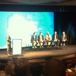
I was completely ready for some high-up from Facebook to come out and talk about how they are ready to deploy ARM-based datacenters but it was not to be. That had been my prediction at the start of the keynote to Dan Nenni who was sitting beside me.