Metastability is an inescapable phenomenon in digital electronic systems. This phenomenon has been known to cause fatal system errors for half a century. Over the years, designers have used convenient rules of thumb for designing synchronizers to mitigate it. However, as digital circuits have become more complex, smaller and faster with reduced voltage, these rules of thumb are beginning to fail. A new tool from Blendics, MetaACE, has been developed that accurately evaluates metastability failures in contemporary SoCs.
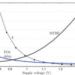
A synchronizer settles to a valid output voltage in period of time that is without an upper bound. This settling-time regime is largely exponential with a time constant t. Throughout a number of the past semiconductor process generations, t has been proportional to FO4 delay and decreased in every generation, thus providing better synchronizer performance at each generation. However, a change in the relationship between t and FO4 delay has emerged at process geometries of 90 nm and below. Operating conditions and process variations further aggravate the situation and can cause many orders of magnitude variation in the MTBF of a synchronizer. As a result, traditional guidelines for synchronizer design are no longer adequate. To illustrate how these traditional rules of thumb fail, Figure 1 shows the effect of supply voltage on t and, in turn, on MTBF.
Figure 1. Settling time-constant τ, FO4 delay and MTBF as a function of the supply voltage (V) for a 65 nm CMOS synchronizer operated with a 200 MHz clock.
Note that t varies by almost an order of magnitude more than does the delay through an FO4 inverter. An equivalent increase in transistor threshold voltage Vth produces the same difference between the FO4 delay and t. Such an increase in Vth can occur under low temperature operation of the synchronizer. The combination of low supply voltage and low temperature can lead to sub-second values of MTBF and an almost certain system failure.
It would be advantageous to be able to predict synchronizer performance before fabrication. This would aid the designer in building a reliable, but not over-designed synchronizer (over-design adds area and latency to an otherwise reliable design). Blendics has developed a software system, MetaACE, that accurately predicts synchronizer MTBF.
Simulating a synchronizer can provide the essential parameters intrinsic to a particular semiconductor process, but more information is needed to estimate the MTBF of the circuit in a particular application. Extrinsic parameters such as clock period, clock duty cycle, rate of data transitions and number of stages in the synchronizer depend on the application and not on the semiconductor process. The MTBF for these various applications of a synchronizer design can be calculated given the intrinsic parameters, however. Figure 2 compares the calculated and simulated results for 2, 3 and 4 stage flip-flops for various clock periods and a data transition rate of 200 MHz.
Figure 2. Comparison of calculated and simulated estimates of MTBF.
It is clear from Figure 2 that there are extrinsic conditions under which even a 2 flip-flop synchronizer at a nominal supply voltage and temperature is unreliable. At a 1- nsec clock period, a typical double-ranked 90 nm synchronizer’s MTBF is less than a year and probably inadequate. Increasing the number of stages to four increases the MTBF to about 1010 years; more than adequate for most cases.
Manufacturers of mission critical products should carefully consider the risk of synchronizer failure and take the necessary steps so that their engineers and their semiconductor vendors will insure a satisfactory MTBF over a system lifetime, particularly when human lives are at risk.
About the Author
Dr. Jerome (Jerry) Cox, President, CEO and Founder, Blendics
Jerry received his BS, MS and ScD degrees in Electrical Engineering from MIT. From 1961 to 1973 he introduced small computers to biomedical research and participated in pioneering research in asynchronous computing. From. 1974 to 1991, he was chair of the Washington University CSE Department and in 1997 became founder and Vice President for Strategic Planning for Growth Networks. This venture-funded, chip-set company sold to Cisco in 2000 for $350M and eventually led to the top-of-the-line Cisco router, the CRS-1. Over his professional career he has taught and done research in computer architecture, medical imaging, statistical estimation theory and medical signal analysis. He has designed and built many digital systems, using both the synchronous and asynchronous approaches. He has published over 100 scientific papers and book chapters and has ten patents.
lang: en_US