With the insatiable wafer appetites of the fabless semiconductor companies in the mobile space, yield has never been more critical. The result being better EDA tools every year and this blog highlights one of the many examples. It has been a pleasure writing about Solido Design Automation and seeing them succeed amongst the foundries and their top customers. Here is a Q&A with Amit Gupta, president & CEO of Solido, to get more details on the new Solido Variation Designer 3.0 release:
Q: What is Solido Variation Designer used for?
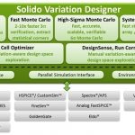
Solido Variation Designer is variation analysis and design software for custom ICs. Our users run Variation Designer to achieve maximum yield and performance on their designs. It boosts SPICE simulator efficiency while increasing design coverage.
Q: Who are the customers of Solido Variation Designer?
Variation Designer is being used by the world’s top semiconductor companies and foundries to design memory, standard cell, analog/RF and custom digital designs at leading design nodes including TSMC, GLOBALFOUNDRIES and Samsung 130nm, 90nm, 65nm, 40nm, 28nm, 20nm, 16nm and 14nm.
Q: What specific customer challenges does Solido Variation Designer 3.0 address?
Variation Designer 3.0 is based on user input from a wide range of semiconductor companies designing anywhere from 130nm to the most advanced process nodes. In general, we are seeing our customers increasingly being hit by variation issues resulting in sub-optimal performance and yield compared to what the manufacturing process allows for. Variation Designer 3.0 gives our users the ability to address the following:
- PVT corner design.PVT variation includes process (e.g. FF, SS, FS, SF, TT model corners that can be device specific), voltage, temperature, load and parasitic based variation. When taking all the combinations of these parameters, our customers end up having 1000s or 10,000s of corner combinations to simulate. The challenge is that to simulate all the corner combinations is accurate, but very slow. Guessing which corners to simulate is faster but inaccurate.
Our customers use Solido Variation Designer Fast PVTto automatically figure out which are the worst case corners while simulating only a fraction of the corner combinations. This results in far fewer simulations than brute force PVT corner analysis without compromising accuracy.
- 3-sigma Monte Carlo design. The process model corners that foundries like TSMC, GLOBALFOUNDRIES and Samsung release in their PDKs are not well-suited to individual designs. They are either overly conservative leading to overdesign, or overly optimistic leading to yield loss. Consequently, foundries are now releasing local and global statistical variation models for designs to run Monte Carlo analysis simulation on their designs. However, brute force Monte Carlo SPICE simulation is slow, inefficient and time consuming.
Our customers use Solido Variation Designer Fast Monte Carlo to cut down the number of simulations to achieve 3-sigma design without compromising accuracy, and to extract design specific 3-sigma corners to design to.
- High-sigma Monte Carlo design. To design to 6-sigma, 5 billion Monte Carlo sample simulations would be needed, which would take years and is therefore impractical. Alternatively, designers are designing to 3-sigma and extrapolating to 6-sigma, but this methodology is inaccurate. Some companies have developed internal importance sampling techniques, but these don’t scale and suffer from accuracy issues.
Our customers use Solido Variation Designer High-Sigma Monte Carlo to get the 5 billion Monte Carlo accuracy runs in only a few thousand simulations.This is a dramatic reduction in SPICE simulations and improvement in design coverage. Solido High-Sigma Monte Carlo is fast, accurate, scalable and verifiable. Example designs being run include memory bit cells, memory sense amps, memory columns/sub-arrays, analog designs (e.g. SerDes, Data Converters), and standard cell library designs (e.g. flip-flops).
- Variation debug. If the design is failing PVT corners, 3-sigma or 6-sigma Monte Carlo verification steps, designers need to identify the design sensitivities to variation and figure out how to fix the design, making it robust to variation. Manually changing the device sizes and running PVT or Monte Carlo analysis to check whether the changes fix the design is tedious and time consuming.
Our customers use Solido Variation Designer DesignSense to automatically identify design sensitivities to variation, which enables them to quickly make necessary design changes and verify that it’s meeting specifications.
- Cell optimization. Similar to variation debug where the design is failing PVT corners, 3-sigma or 6-sigma Monte Carlo verification steps, or the design is not optimized against spec, changing device sizes and running PVT or Monte Carlo analysis to check whether the design is optimal is also tedious and time consuming.
Our customers use Solido Variation Designer Cell Optimizer to automatically vary device sizes within any design and PDK sizing constraints, to optimize the design against PVT and 3-sigma to 6-sigma Monte Carlo variation.
Q: How have your customers deployed Solido Variation Designer in their production flows?
Solido Variation Designer has been established in the signoff flow of most world leading semiconductor companies and foundries.
Users input designs into Solido Variation Designer through the integration we have with Cadence Virtuoso Analog Design Environment or simply by feeding it a netlist. Variation Designer then automatically iterates with the user’s SPICE simulator (we integrate with Cadence Spectre/APS, Synopsys HSPICE/XA/HSIM/FineSim, BDA AFS, Mentor Graphics Eldo and Agilent GoldenGate) to run Fast PVT, Fast Monte Carlo, High-Sigma Monte Carlo, DesignSense and Cell Optimizer tasks. We also support all PDKs that contain process corner or Monte Carlo variation data, and we are qualified by various foundries like TSMC and GLOBALFOUNDRIES.
Some example benefits our customers have seen after adopting Solido Variation Designer:
[TABLE] border=”1″
|-
| style=”width: 121px” | Solido Variation Designer App
| style=”width: 113px” | Customer Design
| style=”width: 180px” | Customer Challenge
| style=”width: 225px” | Benefit of adopting
Solido Variation Designer
|-
| style=”width: 121px” | Fast PVT
| style=”width: 113px” | 28nm DAC
| style=”width: 180px” | 1215 corners takes too long to run, guessing which are worst-case is error prone, no standardized methodology.
| style=”width: 225px” | Correctly found worst-case corners for all outputs in only 296 simulations (4.1x simulation reduction), standardized on Solido Fast PVT methodology.
|-
| style=”width: 121px” | Fast Monte Carlo
| style=”width: 113px” | 20nm folded cascode amplifier
| style=”width: 180px” | 3000 Monte Carlo simulations takes too long to run, running only 100 Monte Carlo simulations doesn’t verify to 3 sigma, no standardized methodology.
| style=”width: 225px” | Verified to 3 sigma in only 300 simulations (10x simulation reduction), standard on Solido Fast Monte Carlo methodology.
|-
| style=”width: 121px” | High-Sigma Monte Carlo
| style=”width: 113px” | 16nm memory column
| style=”width: 180px” | Verifying to 6-sigma would take 5 billion simulations which is impractical, extrapolating to 6-sigma is inaccurate.
| style=”width: 225px” | Verified to 6 sigma in only 4500 simulations, run was fast, accurate, scalable and verifiable, standardized on Solido High-Sigma Monte Carlo methodology
|-
| style=”width: 121px” | DesignSense
| style=”width: 113px” | 40nm comparator
| style=”width: 180px” | Determining device sensitivities to PVT corner and statistical variation difficult, no standardized methodology.
| style=”width: 225px” | Automatically determined device sensitivities to variation, making the design robust to variation, standardized on Solido DesignSense methodology.
|-
| style=”width: 121px” | Cell Optimizer
| style=”width: 113px” | 28nm flip-flop
| style=”width: 180px” | Optimizing specifications across PVT and statistical variation is time consuming and uses too many simulations.
| style=”width: 225px” | 24.1% improvement in flip-flop setup time performance in only 2.75 minutes, standardized on Solido Cell Optimizer methodology.
|-
Q: What’s new in Solido Variation Designer 3.0?
Lots, this is Solido’s biggest release ever. Highlights include:
- Significantly increased capacity
- New features, enhancements and performance improvements in every application
- Re-engineered GUI and full command-line interface for all apps
- Expanded simulator support and third-party tool integration
Q: What detailed features did you add to Solido Variation Designer 3.0?
Solido Variation Designer 3.0 Fast PVT enhancements:
- Increased capacity by 10x
- Support for custom string-based variables in the netlist
- 2D scatterplots
- Interactive impacts
Solido Variation Designer 3.0 Fast Monte Carlo enhancements:
- Faster 3-sigma verification with density-based stopping
- “Simulate-and-predict” mode for up to 20x faster 3-sigma runtimes
- Improved accuracy and robustness of density estimates
- Enhanced results visualization when running multiple corners
- Verified capacity increased by 10x for both number of devices and number of samples
Solido Variation Designer 3.0 High-Sigma Monte Carlo enhancements:
- 20x faster algorithms for large designs
- 10x increase in variable capacity
- Process variable impacts
- Support for binary and multi-modal output measurements
- Support for high-sigma global+local analysis
Solido Variation Designer 3.0 Cell Optimizer enhancements:
- Improved, faster cell optimization algorithm
- Support for Spectre netlists
Solido Variation Designer 3.0 integration enhancements:
- Mixed-language netlist support
- Spectre netlist-in support
- Support for Agilent GoldenGate
- Native Mentor Graphics Eldo support
- Runtime Design Automation NetworkComputer support
- Faster, more scalable, and more robust Cadence Virtuoso ADE integration
Solido Variation Designer 3.0 general enhancements:
- Up to 100x faster load times on large circuits/netlists
- Way better performance with large Cadence designs; especially extracted views
- Re-engineered, even more responsive GUI
- New command-line interface for all apps
- New report generation system with customizable templates
- Re-designed, more robust netlist parser
- Updated and more comprehensive documentation
- TSMC 16nm / TMI2 support
- Hundreds of minor quality, reliability, usability and performance improvements
Q: How can our readers get more information?
You can visit our website at www.solidodesign.com for more information. You can also contact us at info@solidodesign.com for an in-person or WebEx demo.
lang: en_US