You are currently viewing SemiWiki as a guest which gives you limited access to the site. To view blog comments and experience other SemiWiki features you must be a registered member. Registration is fast, simple, and absolutely free so please, join our community today!
Formal verification methods are being adopted at a fast pace as a complement to traditional verification methods like functional simulation for IP blocks in SoC designs. I had a video meeting with Max Birtel, co-founder of LUBIS EDA and learned more about their history, products and vision. This company started recently in 2020 to bring formal products to market, based on their experience providing verification services and then productizing their formal apps.
Their vision is to automate formal verification, which reveals hard to find bugs and makes high risk silicon designs more reliable. With a team of 35 people based in Germany, they provide expert training and support through consulting and a formal bootcamp, plus their technology provides automated setup and SVA assertion generation, finally with automated verification it simplifies complex bug detection with AI-driven tools.
VIP has been customized for common designs like RISC-V and AMBA protocols. They even have a cloud-based product, dubbed LUBIS-on-cloud, which means no software to install. In 2023 the company completed over 50 projects, with more than 250 bugs reported, taking typically under 30 days per block. Common blocks like limiters, memories and arbiters required 10 to 25 days. Control logic like AXI to X, routers and CHI took 25 to 50 days. Caches that were pipelined or RMW were validated in 25 to 40 days. Compute cores – Crypto, RISC-V, Image and Tensors took 10 to 50 days.
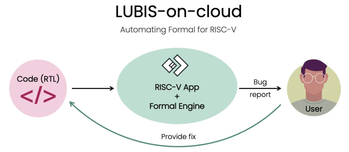
The LUBIS-on-cloud product takes your RTL code, then runs an App that controls a formal engine (Cadence, Siemens, Synopsys), which produces a bug report that a verification engineer reviews to finally make bug fixes. Here’s the flow for verifying a RISC-V processor, which takes very little training or experience with formal tools. You would see your first bug report within an hour.
An example open-source RISC-V processor was uploaded, setup was automatic, then the App was run to start formal verification. Bugs were reported and details of the bug displayed, so that an RTL engineer could find and fix the bug. There were even waveforms shown to help in the debug process. AI is used to explain the bug in English, speeding the debug.
AI Debug
Using these apps to control the formal engines makes it easier for an un-trained engineer to use a formal approach, shortening the verification effort.
Cloud Demo
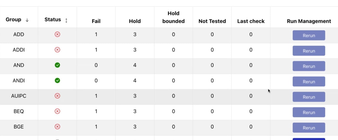
It was refreshing to see a live EDA demo on a RISC-V processor, and login was with Microsoft. The first run of the formal app revealed that 5 bugs were found.
Status of formal runs
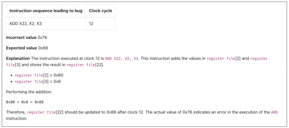
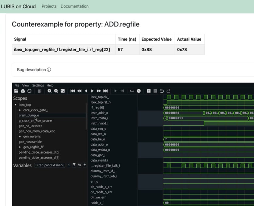
Max clicked on a bug to see why the run had failed, and it reported which signal had a mismatch between expected and actual values, along with waveforms.
Bug report details
For this block the test failed within 2 minutes, and the tool provides the counter example. You can either debug with the provided waveforms or choose to download the SV testbench to replicate the bug in your own UVM environment. An engineer still must manually fix the bug, then re-run the formal app until it passes to complete verification.
Summary
The focused engineering group at LUBIS EDA has made using formal verification tools quite automated and easy to use with the app approach, and the AI-based debug report really makes understanding what caused the bug explicit. Evaluating the cloud-based tool looks straight forward and intuitive
I also discovered where the company name LUBIS came from, it’s a mixture of the founder’s names: Ludwig, Bittel, Shwartz.
As usual in January we start with a look back at the papers we reviewed last year. Paul Cunningham (GM, Verification at Cadence), Raúl Camposano (Silicon Catalyst, entrepreneur, former Synopsys CTO and lecturer at Stanford, EE292A) and I continue our series on research ideas. As always, feedback welcome.
The 2024 Picks
These are the blogs we posted through the year, sorted by popularity. We averaged 12.6k engagements per blog, a little up from last year; thank you for your continued interest! The leader at over 17k views was a surprise, using automated theorem proving to validate multipliers. While still an exotic technology more commonly at home in proving math theorems (the 4-color problem) and the security of specialized OSes, it seems our readership is more than intrigued, perhaps looking for future methods to extend formal verification?
Wow! 5 years of blogging our appreciation for innovation in verification. And our readership continues to increase every year. I never expected this. Thank you, readers!
Our most recent paper, picking up on research by MIT on accelerating logic simulation (see here), had the most hits out of the gate in its first month. This was a great paper, and I hope MIT continue active research in this area. Our blog on State Space Models (see here) was second out of the gate. It didn’t expect this but am delighted to see it as I also found the work very intriguing, especially the structural parallels between an SSM and control vs. datapath in a digital circuit.
The paper on using theorem proving techniques rather than SAT/BDD for multiplier correctness proofs (see here) was also somewhat of a surprise hit for me, but another happy surprise. While the content was heavy, the paper was very well written, and I suspect popular because it is relevant to the verification of AI accelerator chips.
After these top 3 winners we have a mix of hits in the 9-14k range, which still means a lot of interest in every paper we blogged on. I was glad to have read the compiler tuning paper (see here) as it confirmed the same sorts of finding we have been seeing internally at Cadence.
Looking forwards to this year, we would welcome your feedback and suggestions on what to cover. AI, accelerated simulation, and formal will all continue to be important topics – I see the same high interest in these topics from our Cadence customers. Another area which is getting increasing attention in the commercial world is “synthetic content”. This is verification done by generating interesting bare metal software programs that run on the chip being verified and attempt to stress test correctness and performance in clever ways. Synthetic content sits somewhere between signal level testbenches in, say SystemVerilog UVM, and true system-level testing running an actual operating system and application software. We’ll try to cover this topic some more in 2025. Looking back on 2024, we didn’t look at mixed-signal verification. We aim to pay more attention to this area this year.
Raúl’s view
Surprisingly, Wine Spectator named a Chilean wine as their #1 pick for their 2024 list. Similarly, our readers surprisingly selected a paper on theorem proving for verifying multipliers as the most-viewed blog post of 2024. However, the broader trend tells a different story. While the wine list remains dominated by familiar regions, our reviewed papers, much like last year, were largely focused on AI in verification. Over half of the papers we covered dealt with AI-related topics.
The second most-viewed paper, Mamba, diverged from verification entirely. It explores a promising architecture based on SSM, which shows promise as a potential alternative to Transformers, particularly for applications requiring efficient processing of long sequences. Meanwhile, AI applications in verification occupied spots 6, 7, 8, 10, and 11. This might suggest a degree of reader fatigue with these themes or perhaps a sense of saturation in the field. To list them:
Detecting transient faults in DNN accelerators using AI and RTL simulation.
Using Bayesian optimization to optimally configure compiler flags.
Leveraging large language models (LLMs) for fault localization in Java programs.
Applying neural networks to identify coverage “holes.”
Employing deep neural networks (DNNs) to enhance functional safety in image classification.
The remaining papers were Verification- or EDA-specific and captured considerable interest. Ranking third was a paper on accelerating RTL simulation using a dedicated HW/SW architecture (SASH). Fourth place went to a practical approach for speeding up fault simulation, while fifth focused on leveraging fuzzing for NoC verification. Ninth place featured a study on managing BDD size for floating-point adder verification—a second formal verification paper, though surprisingly, it was among the least viewed.
As I look ahead to a fifth year of blogging about verification papers, I’m curious to see which topics we’ll explore based on your feedback. The continued growth in readership is especially encouraging—our 2023 retrospective saw a 40% increase in readers compared to the previous year. Thank you for your interest!
Noise minimization is required for advanced analog and radiofrequency (RF) circuits. Unlike digital circuits, where noise is a second-order effect, system performance metrics such as signal-to-noise ratio (SNR), phase noise, timing jitter, and bit error rate (BER) are directly affected in analog and RF designs. Effective design optimization in the presence of random device noise is challenging because the noise sources are inherent in the circuit elements and cannot be eliminated. Since device noise determines the fundamental limits of circuit functionality, it plays a significant role in analog/RF circuit development.
Noise related issues become particularly critical in circuits with noise-sensitive architectures, tight specifications, and implementation in nanometer CMOS processes with low voltage levels and high frequencies. Most common complex blocks, including analog-to-digital converters (ADC), phase locked loop (PLL), delay locked loop (DLL), transmit chains, receive chains, SerDes, and CMOS image sensors, are highly susceptible to noise.
Measuring and verifying random device noise performance for these circuits can be achieved through a verification hierarchy, starting from smaller building blocks (such as switches, filters) with simple and fast linear noise analysis, to moderate-sized blocks (such as voltage controlled oscillator (VCO), amplifiers, integrators, clocked comparators) using more complex RF noise analysis and sometimes transient noise, and finally, complex blocks (such as ADCs, PLLs, Transmitter, Receiver) using transient noise analysis and in some cases RF noise analysis.
This article will focus on the benefits of full-spectrum transient noise analysis as a must-have for sign-off verification. Full-spectrum transient noise analysis enables engineers to achieve silicon correlation for varied circuit types. It has shown excellent correlation over generations of nanometer process nodes within 1-2 dB of silicon measurements for integer-N PLLs, fractional-N PLLs, and delta-sigma ADCs. In addition, engineers will benefit from the ability to confirm accurate full-spectrum transient noise with proven RF noise analyses (e.g., phase noise of a VCO or input referred noise for a StrongArm Latch).
What is device noise?
Noise in semiconductor circuits is generally divided into deterministic and random sources. Deterministic noise is systematic, bounded, and predictable, while random noise is stochastic, unbounded, and not predictable. Device noise is random and can be categorized into two subtypes: white noise and flicker noise.
White noise
White noise is a random signal with a flat spectral density. The primary sources of white noise are thermal noise and shot noise. The main white noise source in analog/RF CMOS circuits is the MOS device channel thermal noise. Thermal noise results from voltage fluctuations caused by the Brownian motion of electrons in a resistive medium. Thermal noise is found in both passive and active devices. It is broadband white noise that intensifies as temperature increases. Thermal noise has a Gaussian amplitude distribution in the time domain, and its power is evenly distributed across the frequency spectrum. Thermal noise dominates in many applications. Shot noise derives from the discrete quantum nature of electron flow through a potential barrier.
Flicker Noise
Flicker noise, also known as 1/f noise, is caused by traps in semiconductors where carriers that would normally constitute DC current flow are captured for some time and then released. Flicker noise process correlation times are exceptionally long, which makes the power spectral density of flicker noise proportional to 1/f.
What is transient noise analysis?
Transient noise analysis simulates a circuit’s response to random device noise (white and/or flicker). It models transistor noise as current sources with random values based on the noise intensity information from the device model (see Figure 1). Since it is statistical based, the accuracy of transient noise analysis is a function of the number of random samples simulated, i.e., the simulation interval.
Figure 1: Random device noise in resistors and MOSFETs
What is full-spectrum transient noise analysis?
Full-spectrum transient noise directly solves the stochastic differential equations to generate random noise sources at each time step, uses standard device model parameters for white and flicker noise, changes the noise intensity with instantaneous bias, and shows excellent correlation with other noise methods (linear noise, periodic noise, sampled periodic noise, etc.) on a wide range of circuits (such as VCOs, switched-capacitor circuits, clocked comparators, dividers).
Comparison of transient and transient noise signals
Transient analysis is a ubiquitous verification method for a broad range of circuit types, including digital, memories, analog, image sensors, and RF circuits. It is also utilized for measuring deterministic noise, such as power supply-induced noise. However, transient does not include device noise. To account for device noise, we must run transient noise.
The difference between a transient and a transient noise simulation can be dramatic and significant to a design’s overall performance. Both PLLs and ADCs have metrics to compare noise performance. For ADCs it is signal-to-noise ratio (SNR) and for PLLs it is either Phase Noise or timing jitter. Refer to figures 2 and 3 below to note the drastic difference between transient and transient noise.
The ADC Power Spectral Density (PSD) shown in Figure 2 is a 4th order Delta-sigma ADC measuring the SNR, a common metric for noise performance. There is a ~38 dB difference between the transient and transient noise SNR.
Figure 2: 4th order Delta-sigma Analog-to-Digital Converter (ADC) – transient vs transient noise
The PLL phase noise shown in in Figure 3 is from an Integer-N Phased Locked Loop (PLL) with the VCO operating at 10 GHz and used in a wireline transceiver. There is a 10 dB difference between the transient and transient noise Phase Noise.
Figure 3: Transient vs transient noise of 10 GHz Integer-N PLL
Proper methods to setting up and running transient noise
To achieve accurate noise results running transient noise, it is imperative to properly set the SPICE accuracy, noise parameters (noisefmin, noisefmax), stop time, and apply proper post-processing methods. It is not within the scope of this article to go through a detailed explanation of all the parameters, option settings and post-processing steps. The example below (see Figure 4) shows the steps to setup, simulate, and measure PLL Period Jitter to give you a sense of what the process entails.
Figure 4: Example process from setting up to simulating to post-processing for jitter measurement
Why we need to consider confidence intervals when measuring transient noise results
You will notice a label “PhaseNoise_CI” in Figure 3. This stands for the Phase Noise Confidence Interval. The confidence interval measures uncertainty around the phase noise measurement (-139.34 dBc/Hz) at 100 MHz. While running transient noise, we measure a stochastic or random process. Because of this, we cannot simply measure an output such as signal-to-noise ratio (SNR) or phase noise as a single value and report the results, since it does not include the uncertainty of the measurement. As with Monte Carlo simulations, which deal with random process variations, we must also include a confidence interval and confidence level to give us an idea of the uncertainty of the measurement. The confidence interval or uncertainty can be reduced by varying the noise seed in parallel runs.
Below is a table showing an incorrect reporting of measurements for a PLL and ADC. Note that the correct reporting includes uncertainty.
Building confidence in your transient noise results
Transient noise is broadly adopted for various circuit blocks, architectures, and process technologies. However, for the unfamiliar, although it may seem a reasonable approach, designers may be uncomfortable or uncertain of its accuracy and methodology. Several whitepapers and presentations show Siemens Analog FastSPICE (AFS) Transient noise correlation to silicon measurements for both PLLs and ADCs over many generations of process nodes, including FinFET process. This is the most convincing approach.
However, as an alternate approach, comparing different and trusted analysis methods (such as linear noise, PNoise, Sampled PNoise, HBNoise) to transient is a viable approach to build confidence in the results.
Using a common Integer-N PLL we can compare various analysis methods and see if they match. This is a useful circuit as we know the VCO dominates the phase noise at higher offset frequencies above the PLL bandwidth. Because of this, we can measure the phase noise for the following
VCO Phase Noise – running PSS large signal and PNoise small signal analysis, HB large signal /HBNOISE small signal analysis, and transient noise analysis. PSS refers to periodic steady state, also known as Shooting Newton. HB refers to industry recognized Harmonic Balance.
PLL Phase Noise – running transient noise for the closed loop PLL
In figure 5, below we can see all three methods of calculating phase noise for the VCO match very closely. In addition, the closed loop PLL phase noise also matches well with the three phase noise measurements of the VCO. This type of comparison can be achieved for many circuit types including switched-capacitor circuits, clocked comparators, and many others.
Figure 5: Matching phase noise for a closed loop PLL, and VCO
Siemens advances full-spectrum transient noise analysis to its third generation with SolidoTM Simulation Suite
The foundations and first generation of silicon accurate full-spectrum transient noise analysis were developed by Berkeley Design Automation (BDA) and enabled by directly solving the stochastic differential equations for noise, resulting in silicon correlation for ADCs and PLLs within 1-2 dB. Because of its high performance, capacity, and accuracy, it was selected as the sign-off solution for many leading semiconductor companies. This trend continued for smaller geometries down to 40nm in the planar FET nodes. Below 40nm, there was a disruption where the design complexity increased due to more sophisticated FET models, increased parasitics, lower voltages, and higher frequencies. However, upon entering the FinFET era (< 16nm), the complexity of the designs increased by 10x-100x as FinFET models were much more complex for analog simulators. It was no longer feasible to run pre-layout and estimated post-layout designs, resistance, and capacitance (RCC) extractions were required, which resulted in simulation runtimes 10x-20x longer for similar designs.
This trend forced a second generation of full-spectrum transient noise with the release of Analog FastSPICE eXTreme (AFS XT) in 2020. This technology addressed the new demands on circuit designers by maintaining accuracy with up to 10x performance boost over the original AFS implementation.
With the acceleration of process technology now pushing 2nm designs, FET models using Gate-All-Around are more complex, metal resistance has increased over 10x compared to 40nm, and simulation runtime increased by 20x. This has forced another step function to innovate and address designers’ needs for performance, capacity, while maintaining noise accuracy for the smallest geometries. Siemens advanced to its next and 3rd generation of full spectrum transient noise technology with Solido SPICE, part of the Solido Simulation Suite that was launched at Design Automation Conference 2024. Solido SPICE is Siemens’ next-generation, feature-rich SPICE simulation technology, providing a 2-30x speedup for analog, mixed-signal, RF and 3D IC verification. With newer convergence, cache efficient algorithms and high multi-core scalability, Solido SPICE provides a significant performance boost for large pre- or post-layout designs. RF IC developers can directly benefit from Solido SPICE’s new RF verification capabilities, while multi-die, 2.5D, 3D and memory interface developers can now experience an efficient capability for full channel transceiver verification that includes equalization, drastically reducing interface assumptions and accelerating verification.
This article discusses the significance of full-spectrum transient noise analysis in the design of advanced analog and RF circuits, emphasizing its necessity for achieving silicon success. An introduction of noise in analog and RF circuits set the foundation for understanding device noise and how it is captured when running transient noise. Methods were shown to compare transient noise results to various RF methods achieving excellent correlation. We concluded with the progression through three generations of full-spectrum transient noise, ending in the most advanced implementation available in the Siemens’ Solido Simulation Suite.
Authors:
Scott Guyton – Director of Solutions Architecture, Custom IC Division
Pradeep Thiagarajan – Director of Product Management, Custom IC Division
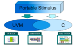
In the early days of the PSS rollout, some verification engineers were suspicious. Just as they were beginning to get comfortable with UVM, here came yet another standard to add to their learning and complexity overhead. Then the fog started to clear; UVM is ideal for block-level testing whereas PSS is ideal for system level testing. And the “P” in PSS is critical. UVM tests are portable into PSS test frameworks as are C tests running on a processor. All that effort put into developing detailed high coverage tests at the block level pays off also at the system level. Of course there should be some interoperability planning between the three test frameworks (PSS, UVM, C) but that was always the intent behind the standard. Siemens EDA have just released a white paper explaining how they recommend such a collaboration.
System-level test scenarios
Why can’t this all be handled in UVM with suitable sequences and randomization? Because what you need to test is simply too high-level and distributed to capture meaningfully in block-centric UVM sequences. Consider for example a multi-core processor cluster supported by coherent cache. Each processor is handling some task, and each is reading from and writing to memory through the cache. Which in turn must ensure a read access to any given logical address must return a consistent current value for that address, even if there is a pending (write) update to the same address from another processor.
Point being that behavior to be tested is distributed across multiple processors, caches (L1s and L2 for example) and a coherent NoC, already a complex state space. And when you build tests for such a system, you must account for factors which are meaningful in this sort of test: checking compliance with the expected coherence protocol (eg MOESI), handling write-through, accumulating stats for cache misses, detecting false sharing and so on. All very feasible in PSS but accommodating this would break your brain in UVM. Then randomization must randomize appropriate scenarios of read and write activity from the cores and cacheline states. While trying to break the protocol and memory consistency by stressing reads from/close to logical addresses for which writes are recent or pending.
There are many other system-level testing requirements: checking IO coherency, power management, interrupt handling, and more. All require modeling and randomizing synthetic or semi-real test scenarios running across distributed functions in a subsystem or system.
Folding in UVM and C
PSS is perfect for building and randomizing scenarios at this level, but these still must be connected to DUT-level testbench components. PSS orchestrates running detailed testing through connections to UVM virtual sequences or high-level C models, allowing you to easily coordinate between UVM and C components and to switch to alternate representations where appropriate as the design evolves. It can also help with testing on hybrid platforms, mixing software simulation, emulation and prototyping.
The white paper illustrates the application of their proposed approach with a couple of examples. The first shows a test methodology to verify writing and reading control/status registers in a block under control of a C routine running on a CPU, observing the interaction of register updates/read from the CPU with block functionality. This would be useful in testing development of a driver for example.
The second example outlines how you might build a VIP to test a DMA. While the previous case can also benefit from PSS randomization, this DMA example is a particularly obvious example of the advantages of a PSS approach. Activity between peripherals, memory and CPUs is unpredictable so randomization is especially important to explore traffic options and potential for collisions, starvation, etc. and to determine whether mechanism to mitigate such problems work effectively.
Nice paper. You can get access to the white paper HERE.
Predictions in technology adoption often hinge on a delicate balance between technical feasibility and market dynamics. While business considerations play a pivotal role, the technical category reasons for the success or failure of a prediction are more tangible and often easier to identify—if scrutinized with care. However, over-exuberance and a tendency to overlook these technical realities frequently lead to inaccurate forecasts.
Abhijeet Chakraborty, Vice President of Engineering at Synopsys gave a keynote talk at the Chiplet Summit 2025. His presentation titled “Accelerating AI Chip Development with 3D Multi-Die Designs” closed with a Synopsys prediction of 50% of new chip designs in the HPC market being multi-die by the end of 2025.
A situational analysis may help us get comfortable with that prediction and why the present moment is uniquely suited for widespread adoption of multi-die design implementations. I chatted with Shekhar Kapoor, Executive Director, Product Management at Synopsys to gain additional insights for this purpose.
The Hurdles of Multi-Die Solutions in the Past
Multi-die solutions have long promised improved performance, efficiency, and scalability over monolithic chip designs, but their adoption was historically constrained by technical and economic challenges. Immature interconnect technologies lacked the high bandwidth and low latency needed for seamless communication, while thermal management struggled with heat dissipation from closely packed high-performance components. Power delivery was another hurdle, as stable, efficient supply systems for diverse die requirements were underdeveloped. Additionally, rising interconnect densities led to signal integrity and electromagnetic interference (EMI) issues.
Standardized chiplet interfaces were absent, limiting design flexibility and cross-vendor compatibility. Economically, advanced packaging methods like interposers and 3D stacking were costly and lacked scalable supply chains. Moreover, testing and validation complexities added to development costs and time-to-market delays.
How the Hurdles Have Evolved
Advancements in technology and industry collaboration have resolved many barriers to multi-die solutions. High-speed interconnects like through-silicon vias (TSVs) and silicon interposers now enable efficient, low-latency communication, while open standards like UCIe enhance interoperability across vendors.
Thermal management has improved with advanced cooling techniques and optimized packaging designs, ensuring reliable operation even in 3D-stacked configurations. Power delivery challenges have been addressed with sophisticated management systems, enabling stable and efficient power for diverse dies.
The Benefits of Multi-Die Solutions
The benefits of multi-die solutions are transformative, addressing many of the limitations of traditional monolithic designs. By integrating multiple dies within a single package, these architectures achieve higher performance through improved interconnectivity and reduced latency. Design flexibility is another key advantage, allowing heterogeneous components such as processors, accelerators, and memory to be combined and optimized for specific workloads.
From an economic perspective, multi-die architectures provide a cost-effective path forward as semiconductor nodes approach their physical and economic limits. Smaller dies manufactured on mature nodes can be combined using advanced packaging, reducing costs while maintaining high performance. This modular approach also improves yield and scalability, facilitating faster development cycles and enabling the rapid adoption of emerging technologies.
Why the Timing Is Right for Multi-Die Solutions
The adoption of multi-die solutions is primed for takeoff, driven by technological advancements, market demand, and economic pressures. Applications like AI, high-performance computing, and data analytics require scalable, energy-efficient architectures, which multi-die designs provide. Mature interconnect, thermal management, and power delivery technologies now enable high-volume production, while standardized interfaces like UCIe foster collaboration and reduce costs.
Rising process node costs further underscore the economic value of multi-die solutions, as demonstrated by industry leaders AMD, Intel, Microsoft and NVIDIA in their flagship products. These architectures align with market demands and sustainability goals, offering a cost-effective path to high performance.
Additionally, ecosystem growth fueled by robust supply chains, tools and IP has simplified design and integration, enabled reduced costs and accelerated time-to-market for multi-die systems. Synopsys’ 3DIC Compiler, 3DSO.ai, and Die-to-Die IP are examples of such tools and IP, to name a few.
Summary
The evolution of multi-die solutions represents a turning point in semiconductor design. With significant advancements in interconnect technology, thermal management, power delivery, and ecosystem development, these architectures are now more feasible, efficient, and cost-effective than ever before. As the demand for high-performance, energy-efficient computing grows, multi-die solutions offer a scalable path forward for the semiconductor industry. Positioned at the intersection of technological innovation, market demand, and economic necessity, multi-die solutions are set to play a pivotal role in shaping the future of computing.
The bold prediction by Synopsys of 50% of new HPC chip designs being multi-die implementations in 2025 looks realistic if not bold enough.
A growing trend in system design is the use of multiple ICs mounted in advanced packages, especially in high-performance computing and AI. These modern packages now integrate multiple ICs, often with high-bandwidth memory (HBM), resulting in hundreds of thousands of connections that need proper verification. Traditional methods, often relying on manual processes and spreadsheets, simply cannot keep pace with this complexity. This blog post will explore how a new approach using formal verification is transforming the way IC package connectivity is verified, drawing insights from a recent white paper by Siemens EDA detailing the Innovator3D IC tool flow.
The Challenges of Modern IC Package Design
Historically, IC package design was relatively simple, mainly involving fanning out die bumps to connect to a printed circuit board. However, with heterogeneous integration and advanced packaging technologies, the task has become a complex system integration challenge. Substrate designers now juggle multiple inputs, often from multiple engineers developing their components simultaneously, and must ensure both electrical and functional correctness. The sheer number of connections, often exceeding 500,000, makes manual verification impractical, and relying on spreadsheets becomes error prone and tedious. The maximum number of rows in Excel is 1,048,576 which is not enough for many designs.
Limitations of Traditional Verification Methods
Traditional verification methods are struggling to keep up. Functional verification, which simulates the design to ensure it operates correctly, is challenging for package designs. It requires functional models for each die, models for discrete components, and testbenches. When chiplets, such as HBM, are involved, these models may not be readily available, and even if they are, package designers often lack the expertise to adapt and use them.
Layout versus schematic (LVS) verification, while helpful in ensuring the physical implementation matches the source netlist, does not verify the functional correctness of the design. It can catch shorts and opens, but it cannot confirm that the design works as intended. If the source netlist itself has errors, LVS will not catch them, giving a false sense of security.
Formal Verification: A New Paradigm
Formal verification provides an alternative solution by using mathematical analysis to exhaustively verify all interconnections between IC blocks. This method only requires two key pieces of information:
The system top module with connectivity information
Module port definitions of the dies
Formal verification does not require lengthy testbenches or assertions. It can detect connection errors, ensure the correctness of connections, and identify potential short circuits. Since the method uses mathematical analysis considering all possible stimulus, it can prove connections are correct without any overlooked scenarios.
Innovator3D IC and Check Connect
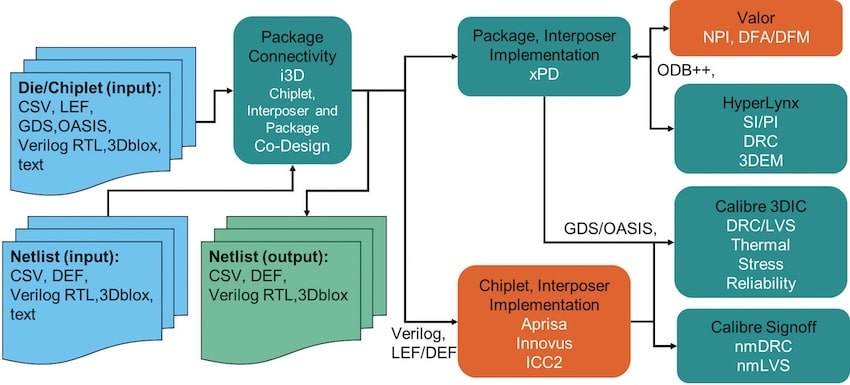
Siemens EDA’s Innovator3D IC (i3D) tool helps engineers tackle the complexities of modern package design. i3D collects data from various sources, such as die, BGA, and netlist data, and allows the creation of system connectivity. The connectivity can be exported in multiple formats, including Verilog, for verification purposes.
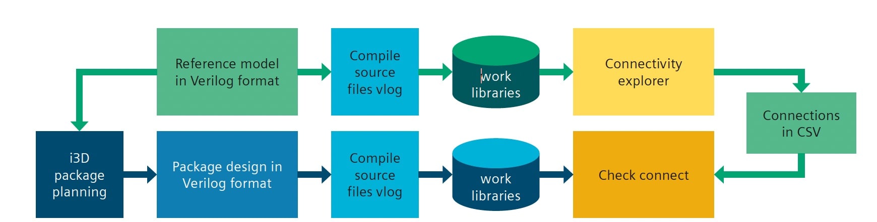
Innovator3D IC flow
Siemens’ Check Connect is a formal verification tool that is used to verify the connectivity of a package design. It uses a golden reference model, often developed by the design team through the design phase and extensive simulation and automatically extracts the connections to verify the design. The tool works with the i3D package design tool to generate Verilog netlists and then verifies the connections. The tool can generate a missing-port report that lists the ports not covered by any connections, helping to identify potential issues in the reference model or the connection specifications. The tool is also very fast and can work on big systems because the design modules are treated as black boxes, focusing only on connections between blocks.
Formal Verification Flow
Benefits of the Formal Approach
Exhaustive Verification: Formal methods mathematically analyze all possible scenarios, guaranteeing that connections are correct.
Early Detection: Errors can be detected early, right after package prototyping, saving time and money.
Automation: The entire flow is automatic, from creating connectivity specifications to verifying packaging output connectivity. The script is simple and can be reused for different projects.
Speed: Automatic parallel algorithms on the compute grid can verify huge numbers of connections in minutes or even seconds. Test cases have shown verification times as low as 30 seconds for designs with over 20,000 connections and 56 seconds for designs with over 40,000 connections.
Improved Reliability: Formal verification is critical in industries with strict regulatory standards, such as aerospace and automotive, because it can provide an exhaustive analysis of connections, and some tools are ISO 26262 certified.
Conclusion
The white paper demonstrates that formal verification is an effective approach for the challenges of modern IC package design. By automating the verification process, it ensures the correctness of connections early in the process, leading to improved quality and reduced time to market. The learning curve for setting up these formal tools takes only minutes. This approach is poised to become an essential part of the modern IC package design flow.
Read the 13 page white paper online showing how Innovator3D IC uses formal verification.
The lifecycle for complex chip design includes many factors. Traditional systems focus on design tasks, associated schedules and manufacturing logistics. While these are important aspects of the project there is a lot more that can be measured, predicted and tracked. Taking a more holistic view of the project opens new opportunities to optimize not only cost and schedule, but sustainability and ecological impact. This expanded view of the chip lifecycle will help to manage critical trends such as water consumption and CO2 emissions.
Innova presented a comprehensive approach to achieve these results in a recent webinar. A replay link is coming but first let’s take a high-level look at how to achieve full flow and resource management visibility to optimize cost and sustainability with Innova.
Dr. Chouki Aktouf presented the webinar. He is a co-founder of Innova Advanced Technologies. Prior to Innova, he founded Defacto in 2003. Before that, Dr. Aktouf was an associate professor of Computer Science at the University of Grenoble – France and leader of a dependability research group. He holds a PhD in Electric Engineering from Grenoble University.
Chouki has a relaxed and easy-going presentation style. He covers a lot of important material clearly and concisely. You will learn a lot from him during this webinar, which is 30 minutes in length followed by a very useful 10-minute Q&A session.
Some Webinar Details
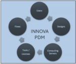
Chouki presents both the software and methodology that are available to achieve big picture management of complex chip design projects and the broader benefits of cost and sustainability that result. At a high level, Innova covers predicting, reporting, optimization and needs for EDA tool licenses, computing server resources, and IP cores which are involved in complex chip design projects
Many benefits of the Innova PDM (Project & Design Management) tool are discussed. In the area of cost reduction, there are two aspects to consider:
Design Flow Management
Report optimal usage scenarios per design project, design flow, etc.
Predict Design Resources
Optimize the usage of computing resources
Design Resource Management
Optimize jobs scheduling with the available design resources
Make cost-effective the debug, reuse and tracking of complex design flows
Correlate between flow execution steps and design resources
Track and manage real-time user-defined alarms
The figure below summarizes the data flow of this approach, which aims to reduce cost by 15 to 30 percent compared to ad-hoc methods.
Innova PDM Flow
Many details are discussed on how to integrate the Innova tools into any design flow. Both GUI and script-based approaches are covered. The use of machine learning to enhance predictability is also covered.
Chouki also discusses in detail how the visibility provided by the Innova flow can help with sustainability considerations, such as carbon footprint. An expanded view of the project is used, which includes aspects such as transportation logistics. The goal is to develop an eco-friendly design footprint.
To illustrate the process, here are some of the items considered. Chouki does a great job explaining how all this works.
Metrics
Flow complexity
Design complexity
Resource complexity
Ecological Impact
Gas emission kgCO2eg
Use of minerals and fossil resources (kgSbeg)
Consumption of primary energy (MJ)
Configuration Recommendation
Flow
Cluster selection according to ecological impact
Chouki illustrates the impact of this type of capability by examining two equivalent design flows with the tool. It turns out the flow that looks more complex on the surface is actually more efficient and significantly more eco-friendly. He points out there is no way to know this without using the kind of detailed management and analysis provided by Innova.
To Learn More
A capability that both optimizes cost and optimizes the eco footprint of a design is critically important for the health of the company and the planet. Innova provides a complete solution, and this webinar explains it very well. I highly recommend you watch the replay. You can access the webinar replay here. And that’s how to achieve full flow and resource management visibility to optimize cost and sustainability with Innova.
Dan is joined by SiLC Technologies CEO Mehdi Asghari. Mehdi is one of the early pioneers of the silicon photonics industry with over 25 years of commercialization experience in this space. SiLC is his third Silicon Photonics start-up focusing on advanced imaging solutions. His previous startups, Kotura and Bookham, both enabled successful exits.
In this informative podcast Dan explores the unique LiDAR technology SiLC is developing with Mehdi, who explains the benefits of Frequency Modulated Continuous Wave (FMCW) technology for LiDAR applications. Mehdi describes a broad range of applications for the technology that all help to deliver accurate, intelligent and robust machine vision. Drone tracking and recognition, diverse mobility applications and warehouse automation and robotics are some of the topics discussed.
The special advantages of SiLC’s technology are discussed along with a view of what lies ahead for the company. The views, thoughts, and opinions expressed in these podcasts belong solely to the speaker, and not to the speaker’s employer, organization, committee or any other group or individual.
High-speed digital (HSD) designers have long tested the limits of realizable speed. GHz frequencies are now the norm, and multi-level signaling is pushing rates higher while the long-awaited transition to optical signaling and even higher rates looms ever closer. Power density is also climbing, and data-hungry applications like AI unexpectedly create bottlenecks in power delivery with decreasing margins on sub-1V power rails carrying thousands of amps into large chips. The demands of signal integrity, power integrity, and electromagnetic interference (EMI) engineering are fueling a new generation of streamlined EDA workflows looking to deliver a high-fidelity, end-to-end digital twin from one simulation environment.
Keysight’s Advanced Design System (ADS) platform has set the industry standard for high-speed digital and power integrity design workflows with in-situ chip and printed circuit board (PCB) EM extraction and simulation. ADS has always prioritized simulation accuracy, combining classic circuit analysis with high-fidelity EM models in a co-simulation approach. It quickly delivers digital twin levels of accuracy, with more detailed results and design insights than extensive physical measurements, which can be challenging to set up, costly, and time-consuming. ADS R&D teams are now breaking new ground with more capabilities to find, visualize, and solve the root causes of complex design failures – before designers commit to hardware.
Keysight EDA teams previewed DesignCon 2025 and Keysight Education Forum technical talks on four design challenges ADS uniquely targets: advanced crosstalk analysis in wide-bus scenarios, 2kAmp power delivery for massive 3DHI chips, analyzing PCIe links with PAM4 modulation, and system simulation and verification of LPDDR5 designs used in AI applications.
One-pass crosstalk analysis for single-ended buses saves costly respins
A simplified view of crosstalk looks at only adjacent lines and judges the goodness of eye patterns. However, Hee-Soo Lee, HSD Segment Lead at Keysight, says customers indicate that tapeouts of dense, high-speed designs fail more often because of complex crosstalk problems – and identifying the culprits can be challenging. “Designing and laying out a complex board with a very wide single-ended bus can be tough, and designers must be mindful of avoiding unwanted design failures due to crosstalk-related eye closure,” says Lee. “Packages and vias on multi-layer boards can inject crosstalk to any victim line, not only from adjacent transmission lines, and with reduced design margin and higher data rates, even 10mV of crosstalk voltage may affect a system’s performance significantly.” If eye patterns look good, there’s no problem, but where and how does a designer go about fixing things if the eye is closed?
“With a 64-bit wide bus, it can be days just manually setting up crosstalk simulation runs,” continues Lee. “Correctly terminating multiple lines is tedious, and one can’t assume terminations are always 50 ohms – it depends on the drivers and receivers and the signaling conditions. One setup gets an answer for one aggressor and multiple victim lines, and then that process needs to be repeated perhaps 150 or 160 times to analyze the entire data bus.” Lee points out that in chip designs, things get even more complicated and can trigger a million-dollar re-spin of die or packaging if the analysis is not done right.
Keysight’s answer is Crosstalk Analyzer, now in the ADS 2025 release, with three unmatched values. First, it uses the IBIS termination model for the drivers and receivers to model terminations accurately, removing the guesswork. Second is the automated workflow for setting up a bus for crosstalk analysis with all aggressors and victims configured. Third are the versatile aggressor modes available, which include rising and falling steps, single pulses, and continuous signals. After this streamlined setup, ADS Crosstalk Analyzer simulates near-end and far-end crosstalk over the entire bus with the correct termination impedances for the signaling context in one pass directly from a single schematic.
“Tools are tools, and we still need engineers to find and fix issues,” adds Lee. He cites a test case from a customer’s example, a board with a memory interface running at 3200Mbps where crosstalk on a line came predominately not from the adjacent trace but from a via farther away, influenced by the BGA package and other vias in the board layout. “We produce meaningful data from automated crosstalk analysis in a few minutes, whereas other error-prone setups can take days and may not highlight the root cause of eye closure.”
Power integrity analysis in 1000A/nsec PCB power delivery network
Speaking of complex packages and multi-layer board layouts with vias, power integrity is also seeing issues stemming from board structure complexity. “Power delivery isn’t DC. It’s AC,” says Heidi Barnes, Sr. Application Engineer at Keysight. “For years, power delivery network (PDN) impedance typically registered as 10s of milliohms. Now, a server-class AI chip consuming 1600W requires PDN impedance in microohms, and suddenly, intentional structures and parasitics in multi-layer PCB and package layouts make a big difference.”
Barnes teams with Steve Sandler of Picotest and Ben Dannan of Signal Edge Solutions to highlight an interesting specimen – a 2000A, 11-bit programmable transient load stepper. Its claim to fame is slewing 1000A of load in one nanosecond. That figure seems otherworldly until one steps back to think about power management and sequencing, rapid switching of many transistors simultaneously, and inrush currents held up by bypass capacitors. It’s more realistic considering today’s large 3DHI chips and the concept of point-of-load power delivery, where rails must enter on some pins toward the center of a package for power integrity, transferred up from lower layers using vias. Barnes helped create a digital twin of the stepper in ADS PIPro for complete EM and electrothermal analysis.
“People may not realize that 10 microohms of impedance on a power rail is sensitive to parasitic inductances of only 100 pH. Now we’re looking at transmission line effects in the kHz range,” continues Barnes. “Validating a power rail for stability used to imply small-signal AC analysis. But to understand these large dynamic loads, with crosstalk and ripple, and where to place things like sense lines, we’re turning to large-signal AC analysis.” Behavioral models of voltage regulator modules (VRMs) traditionally run in SPICE simulators can migrate to ADS frequency domain harmonic balance analysis for large-signal simulations that jump directly to the time domain steady-state ripple solution.
ADS PIPro simulations for this 2kAmp digital twin with 55 VRM phases run in 77 seconds, uncovering and visualizing a resonance from an impedance peak at 91 kHz. “When expensive devices are on the line, like in defense and aerospace applications, engineers need to look at this kind of power integrity simulation to reduce re-spins and prevent inadvertently exceeding a chip’s voltage or thermal reliability specifications,” concludes Barnes.
Pushing PCIe links faster and helping AI chipsets and systems scale
Two more high-speed digital topics look at the evolution of PCIe and the challenge of distributed LPDDR5 interfaces typical in AI applications. Pegah Alavi, Sr. Application Engineer at Keysight, is in a panel session with Samtec, Amphenol, and others, showing recent work with ADS looking deeper at PAM4 modulation used in PCIe 6.0 and other specifications and the impact of channel length and connectors as data rates increase to 128GT/s in future releases. Alavi emphasizes Keysight’s unified measurement science approach, sharing that PCIe compliance test solutions in Keysight real-time oscilloscopes also appear in ADS for use with simulated waveforms. Initial work on PAM4 simulations with 128GT/s data rates is complete, with equalization and channel characteristic enhancements in discussion for future generations of PCIe.
In a separate Keysight Education Forum technical talk, Alavi shares her collaboration with a partner company to develop promising ADS analysis results on power-aware LPDDR5 implementations, finding accurate target Z impedance values for optimizing eye diagrams. “We have a customer designing large AI chipsets, and the punchline is by using ADS, they spotted problems in simulation before fabricating their board prototypes,” she says. Much of the work analyzes trace spacing for crosstalk improvements, but another exciting result is a significant reduction in bypass requirements. “With data in hand, our customer cut bypass capacitors on the board by a bit over two-thirds, from 79 to 25. The analysis reduces BOM costs for the board and improves confidence in design margins for the LPDDR5 buses.”
“Within a single design platform – ADS – combining memory design, signal integrity, and power integrity analysis, we can explore the LPDDR5 design space much more. That will help AI and other 3DHI chipset designs scale faster while delivering first-pass silicon and board success,” Alavi concludes.
Learn more at DesignCon 2025 and KEF
More details will come in tutorial and panel sessions at DesignCon 2025 and the Keysight Education Forum sessions at the Santa Clara Convention Center. In addition to the speaking slots on the program, exhibitor attendees can see Keysight’s ADS with power and signal integrity solutions and its Chiplet PHY Designer in booth #1039. For more information, please visit the following:
Dr Josep Montanyà is a Co-founder leading the company, with +18 years of experience in MEMS, patents and the semiconductor industry. Founded Baolab Microsystems prior to Nanusens.
Tell us a little bit about your company.
We have a patented technology that allows us to build chips with nano-mechanisms inside (called NEMS) using the de facto standard manufacturing for solid state chips (called CMOS). This allows us to have better performance, smaller size and lower cost.
There are many applications for this technology, including sensors, RF tunable devices and even AI processors with higher speeds and less consumption. Our initial focus is on a particular product called RF DTC (Digitally Tunable Capacitor). We have a very clear route to market, with signed LOI, and we will place it into Tier 1 phones (and more) that will hit the market in 4 years.
Beyond this initial product there are more RF devices we can build, and a large variety of sensors. Until now inside each wearable or portable system, you have a digital processor and one or more external sensors chips. We have the capability to change this, by embedding the sensors into the digital processors. Today it is possible to do this by using complex multi-die packages. We don’t need to do that. Instead, at Nanusens, we can build all these sensors monolithically on the same CMOS die where the digital processor is built. And this is done without impacting yield and using minimal additional area. This reduces dramatically the size of the overall system, and it reduces also power consumption to levels that today are unseen.
The company is split between its HQ in Paignton (UK) and a subsidiary in Cerdanyola (Spain).
What was the most exciting high point of 2024 for your company?
This year we got our RF DTC prototype measured by a large corporation. This was a very important milestone, because not only it shows the interest of the industry in our product, but it also validated all our measurements.
These measurements proved the incredible performance that our RF DTC can achieve, and it has helped us to better understand our route to market. Being able to increase by 30% the antenna efficiency of cell phones means that we increase by 30% talk time, we also increase by 14% the range from the base antenna, meaning that many areas of poor reception disappear. And for the smartphone OEM, the size of the PCB can be reduced, given that with our solution there is no need to switch standalone external capacitors. Reducing PCB size inside the phone is a key driver for smartphone OEMs, as this means having more space for battery.
With our chip, we aim to monopolize the +$800m market of smartphone aperture antenna. This is because we have unmatched performance, small size and low cost. And all this comes from the fact that we use our patented technology to build NEMS devices in CMOS.
What was the biggest challenge your company faced in 2024?
Main difficulty for a pre-revenue start-up like Nanusens developing semiconductor and even more MEMS technology is fundraising. Our goal for 2024 on this front was to raise a £8m Series A to provide prototypes of inertial sensor and RF DTC devices, so that next year we would be in the market with our first products, and we have customers waiting for them. This has been moved to 2025 as we will have achieved more significant milestones by then that will facilitate this process.
How is your company’s work addressing this biggest challenge?
We have decided to focus on the RF products, leaving sensors and other devices in our future roadmap. This has allowed us to reduce costs and be more efficient.
What do you think the biggest growth area for 2025 will be, and why?
I think AI processors will keep being the dominant area in semiconductors. The incredible success of NVIDA, plus all the big techs jumping in, forecasts a very interesting year. At the same time, however, the market is starting to adjust itself, and I believe we will start seeing more start-up failures in this field as well. You need something really different to succeed in such a competitive field, dominated by giant players.
How is your company’s work addressing this growth?
We put a limited effort on studying the possibility to build better AI processors using our NEMS in CMOS technology. We discovered that it is possible for us to build vacuum transistors in CMOS. This has the potential to enable x10 faster AI processors and consuming half of the power.
Vacuum transistors enjoy the terahertz range bandwidths of vacuum tubes, but without their problems of large size, mechanical fragility, low reliability and large power consumption. In fact, given the very small, nano-sized gaps of vacuum tubes, there is not even a need for heating the metals at high temperatures. Instead, a low voltage generates such a strong electrical field with this small gap, that electrons fly between the cathode and the anode by field emission.
There are research papers on vacuum transistors, which have been built using custom NEMS processes. At Nanusens, we have the capability to build them using standard CMOS processing. This has the potential to build AI processors far beyond the state of the art, and with a process ready to produce them in high volumes. This is a project for after the Series A round is completed.
What conferences did you attend in 2024 and how was the traffic?
We did not attend any conference this year.
Will you attend conferences in 2025? Same or more?
I don’t know yet. But most probably we will not attend many conferences, as our focus is in internal R+D.
How do customers engage with your company?
Although technically we can sell IP and have already done so, our business model is to sell product (ICs) directly to our customers or through distributors.
Additional questions or final comments?
It is always difficult to predict the future. But 2025 will be a very interesting year. I will be especially interested to see what happens in this race for dominating the AI digital processor market. But, whoever wins this next year, we have a technology that will overpass them in the next years!
Nanusens’ patent pending technology enables MEMS nanostructures to be built within the layers of a CMOS chip using standard CMOS processes. This enables us to create both MEMS sensors and MEMS capacitors with the required control circuitry as innovative, single chip solutions that are significantly smaller than their current, multi-component equivalents. They can also be produced in virtually unlimited numbers in standard CMOS fabs, taking advantage of their low production cost.


