Banner 800x100 0810

Configurable System IP from a Tool Provider

Configurable System IP from a Tool Provider
by Randy Smith on 07-18-2013 at 11:00 pm

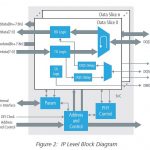
While I have previously blogged on Forte’s Cynthesizer Workbench’s Interface Generator, I want to take another look from a different perspective. Watching the tool and IP together in action through public videos provided by Forte it struck me as odd what I did not consider earlier, on what should have been obvious to me – Forte is not only providing a tool, they are providing validated IP. We expect to see semiconductor intellectual property (SIP) coming from a SIP company such as ARM or Sonics, or from one of the big EDA companies in that market, such as Cadence or Synopsys. But, we do not often see SIP coming from a tool company that is not one of the Big 3.

Why is this important? It is important because one of the best techniques a designer has in improving their productivity is in design reuse and the use of pre-verified SIP. I just wrote a piece about this in another article about the concerns from Bill Dally of nVidia on the need to improve design productivity. Dally laments the time a couple guys could design a chip in a few weeks, a process today that takes 6 months or usually much more. It would seem the key components to get there are to raise the level of abstraction, to dramatically increase the amount of reusable IP, and to adopt a network-on-chip (NoC) architecture to connect the blocks all together. While Dally took this so far as to imply more reusable hard IP, a lot can be gain from pre-verified soft IP if the designers would just stop editing it. It is already verified, so simply leave it alone and take the productivity gains rather than risk the schedule delays and potential bug introductions from trying to improve it.

Another point is to look at the type of IP that Forte is providing – Interface IP. This is in contrast to Forte’s former competitor Synfora whose assets were bought cheaply by Synopsys a bit more than three years ago. Synfora was also a high-level synthesis (HLS) provider which spun-out of Hewlett-Packard. Initially, the company was developing an HLS tool which was tightly coupled with a proprietary processor. That turned out to be a very hard sell. Interface IP provides functions which most every chip can use in different styles of implementation such as point-to-point or FIFO. But a processor is more closely tied to the overall performance of the design and the designers tend to be very familiar with how to use it. The approach Synfora was taking was more like competing with ARM except ARM had a much better ecosystem around its processors. Synfora later abandoned this approach though perhaps too late since a lot of money was burned along the way. In contrast, Forte’s is providing IP to solve problems that come up often but fall into an area where differentiation is not needed. Forte got it right.

To see an example of the Forte Interface IP in action watch the video on their website. The video is well done and runs less than 12 minutes. It should be well worth your time.

lang: en_US


Ajit’s Semicon Keynote

Ajit’s Semicon Keynote
by Paul McLellan on 07-18-2013 at 4:23 pm

The opening keynote to this year’s Semicon West was by Ajit Manocha, the CEO of GlobalFoundries entitled Foundry-driven Innovation In the Mobility Era. It is no secret that mobile applications, especially smartphones and tablets, are the most significant semiconductor market today. It is not just large, it is disruptive. In relatively short periods, companies like Apple, Samsung and Qualcomm have grown enormously, and the PC market, in particular Intel, is suffering and trying to create a successful mobile strategy (or perhaps foundry strategy). The cell-phone market is now bigger than the PC market and in three years should be bigger than the entire PC and tablet markets together at nearly $120B.


Mobile is characterized by short design cycles, a fanatical attention to low power. But the changing features such as bigger screens, higher data rates and thinner form factors make each generation an increasing challenge.

But there is another major change. The cost of ownership of a fab is now so high that only Intel can really afford the investment to keep going with the IDM model. And even they are dipping their toe in the foundry market, most notably with Altera. In 2001 there were a couple of dozen IDMs who had 0.13um fabs. Now in 2013, with work starting on 14/16nm, only GlobalFoundries, TSMC, Samsung and Intel have announced plans. Some later adopters my follow, but the trend is for fewer and fewer companies with the wafer volume to generate the $ required to make a fab a good investment.

Even if you have the money, there are real technology challenges out there. Device architecture with FinFET and FD-SOI and, further in the future, NanoWires and using III-V materials with silicon. On the litho side there are lots of issues with both double patterning (primarily just cost) and EUV (primarily source power at present). I attended the special litho session at Sematech and will be doing a more detailed blog about it soon. But at advanced nodes, both technologies mean that litho will dominate the wafer cost. Lurking in the background is 450mm wafers which will further affect the economies of scale.

Beyond that there is what has now become known as More than Moore, approaches other than two-dimensional scaling of the die. The most obvious technologies here are 2.5D and 3D packaging techniques such as Micron’s memory cube.


Today Manoj believes are moving to Foundry 2.0 which his name for what others have called virtual-IDM. Foundries need to partner for success. They cannot wait until the process is ready and then sit back and wait for designs. It is too slow to get to market and, perhaps more critically for foundries, to slow to get to volume. EDA tools and IP needs to be available well in advance so that customers are ready for volume production ramp at the same time as the fab is.

Foundry 2.0 requires a whole ecosystem of partners (not to mention lots of money) if mobile devices are going to delight and amaze us for the rest of the decade.


Where will Apple Manufacture the next iPhone Brain?

Where will Apple Manufacture the next iPhone Brain?
by Daniel Nenni on 07-17-2013 at 5:00 pm

There still seems to be a lot of confusion here so let me set the record straight. In regards to the Apple Ax SoC, the Apple iPhone 5s will have Samsung 28nm Silicon. Samsung 28nm is still ramping but Samsung can make enough wafers and eat the yield issues no problem. The Apple iPhone 6 in 2014 will have TSMC 20nm as I reported previously. TSMC 20nm is ahead of schedule so no problem there. Contrary to what was reported (TSMC reaches deal with Apple to supply 20nm, 16nm and 10nm chips, sources claim), the iPhone 6s in 2015 will have Samsung 14nm Silicon. Samsung is a bit ahead of the pack on FinFETs and from what I was told they made a wafer price offer that Apple could not refuse. As I mentioned before, there will be a glut of 16/14nm wafers so pricing will be VERY attractive for the fabless semiconductor industry. Best of luck to all who oppose us fabless people, you will need it.

This is all fact. Moving forward is opinion but I have a much better record on being right than my counterparts in regards to the fabless semiconductor ecosystem so keep on reading:

It is being reported that Apple will invest in a fab: Exclusive: Apple has a fab, will make their own chips. This is a complete FABrication. The SemiAccurate website has not even been semi accurate in regards to the foundry business. They have also changed business models so now you have to pay $1,000 to be a member of a rumor website? Good luck with that. I met the site’s owner Charlie Demerjian at CES in Las Vegas two years ago. Lets just say that he may talk tough behind a keyboard but in person, not so much. Charlie was wrong about Apple manufacturing at Intel, he was wrong about TSMC 40nm and TSMC 28nm, and he is wrong here. No way is Apple going to buy into a fab, especially UMC. UMC is a second source foundry which means they are a year or two behind TSMC. The whole point to the fabless ecosystem is competition, the ability to choose wafer providers based on different business variables. No way can Apple/UMC compete with Intel, TSMC, and Samsung on technology and wafer costs. 450mm wafers are coming and Apple will try and compete with a 300mm fab investment?


An article from C/NET has Apple tying up with GLOBALFOUDNRIES:

Apple talking to Globalfoundries about U.S.-based chipmaking, says report. If Apple owned capacity at a fab, it would give the company the kind of control over both design and chip manufacturing that Intel has.

This is not true. Apple started with Samsung as an ASIC customer and has worked for 5+ years to get out from under Samsung and be able to independently participate in the fabless semiconductor ecosystem. Apple does all of their own design work now. Apple even develops foundation semiconductor IP. Apple has successfully moved production from Samsung 28nm to TSMC 20nm. Samsung 28nm is gate-first HKMG technology and TSMC 20nm is gate-last HKMG with double patterning so that change was no small feat. Do a search on LinkedIn for Apple employees under the semiconductor category. You will see hundreds of experienced semiconductor professionals at Apple. You will also see a group of former ATI employees who have recently joined Apple for custom GPU development. Yes, Apple is designing their own GPU.

Bottom line: No way will Apple tie up to one foundry and give up the competitive advantages of the fabless semiconductor ecosystem. Not going to happen. There is a reason why we are all fabless now and I do not see Intel or anyone else turning back time to the Jurassic semiconductor period where “real men have fabs” weighing down their balance sheets, just my opinion of course.


Oasys Bakes a PIE

Oasys Bakes a PIE
by Paul McLellan on 07-17-2013 at 3:01 pm

One challenge in building a modern SoC is that you want to minimize power, performance and area (PPA) while still getting your chip to market on schedule. Realistically, you can’t actually minimize all of these at once since they are tradeoffs: speeding up a critical path often involves upsizing drivers to larger cells which obviously has a negative effect on area and probably on power too. Sometimes you can get into a virtuous cycle where a block gets smaller, and faster and lower power all at once but that is unusual. Some things, like the floorplan, can have a huge impact on the design but precisely what is not really possible to determine without trying it.

In a modern design, especially early on when there is a lot of flexibility in what can be tried, there can be a huge number of possible changes to consider:

  • timing constraints
  • target libraries
  • floorplan, block aspect ratios
  • die size, pin placement, layer assignment
  • voltage reduction
  • power and clock gating modes
  • different RTL coding
  • switch soft IP for hard IP

Oasys’ Parallel Implementation Exploration (PIE) allows designers and architects to perform quick “what if” implementation analysis with minimal effort by varying whichever parameters seem most attractive and automatically run all possible combinations of defined input such as clock frequency, voltage, library or aspect ratio. By lowering the cost of evaluating design options and performing them in parallel allows exploration of a much richer space and so homes in on the best option.

PIE works on existing scripts and is very easy to set up. It runs distributed across multiple CPUs with monitoring capabilities to make it easy to track progress. Reports can be generated in Microsoft Excel for comprehensive analysis of the tradeoffs between the various metrics.


For example, the above graph shows an exploration of a design using 4 different voltages and 4 different frequencies and shows the worst negative slack (WNS) in each case. It is clear that at 1GHz the HVT cells break down and timing is nowhere close to being met.


We can also look at the other two components of PPA, the power and area. We can see that the HVT 0.9V library consumes more power and area than the LVT 0.85V library, because the slower cells require more optimization (higher drive etc) to meet timing and so power and area suffer.

The basic technology of Oasys RealTime Designer optimizes at the RTL level resulting in up to 10X faster turnaround times than traditional synthesis tools. Now, with PIE, design teams can leverage server farms to investigate as many implementations as they want and in just a couple of hours home in on the best implementation.


How to Engage with the Fabless Semiconductor Ecosystem

How to Engage with the Fabless Semiconductor Ecosystem
by Daniel Nenni on 07-16-2013 at 10:00 pm

SemiWiki is absolutely the best place to start of course. You can read observations, opinions, and experiences on a wide variety of semiconductor related topics from semiconductor professionals around the world. You can also mingle with the 653,105+ people who visit SemiWiki in the comment sections and the forum. Registration is FREE and you will not be bothered by pop-up advertisements and such.

Another great place to engage with the fabless semiconductor ecosystem is the GSA:


The Global Semiconductor Alliance (GSA) mission is to accelerate the growth and increase the return on invested capital of the global semiconductor industry by fostering a more effective ecosystem through collaboration, integration and innovation. It addresses the challenges within the supply chain including IP, EDA/design, wafer manufacturing, test and packaging to enable industry-wide solutions. Providing a platform for meaningful global collaboration, the Alliance identifies and articulates market opportunities, encourages and supports entrepreneurship, and provides members with comprehensive and unique market intelligence. Members include companies throughout the supply chain representing 30 countries across the globe. www.gsaglobal.org

In addition to the corporate website, you can follow the GSA on LinkedInHERE. Better yet, you can join one of the LinkedIn groups and engage GSA members directly:

These groups are moderated and populated by industry professionals. Ask questions and you will get answers, believe it.

Of course the best way to engage the fabless semiconductor ecosystem is face to face. The GSA is the best place for this as well. Check their calendar of events HERE. GSA events are excellent for knowledge building and networking. GSA events are also a great place to meet SemiWiki’s Dr. Paul McLellan or myself as we frequent them as well. The food and open bars alone are well worth the trip! GSA also has a YouTube channel with clips from past events HERE.

If your employer is a member of GSA (check HERE to see a member list) you have access to some amazing resources:

The GSA also has a landing page on SemiWiki HERE with expert coverage by Dr. Paul McLellan and myself. Okay, mostly Paul because I’m dieting and the free lunches and dinners with open bars are killing me!

No matter what you read, the fabless semiconductor ecosystem gets stronger everyday. Hundreds of companies and hundreds of thousands of people with a combined budget of hundreds of billions of dollars. There is no stopping us now, believe it.

lang: en_US


Mixed Signal SOC verification Webinar

Mixed Signal SOC verification Webinar
by Daniel Payne on 07-16-2013 at 8:29 pm

When looking at the time to design and verify an SoC we’ve known for many years now that the verification effort requires more time than the design process. So anything that will shorten the verification effort will have the biggest impact on keeping your project on schedule.

A second trend is the amount of Analog content in a mostly Digital SoC, which further complicates the verification process because analog IP is created at the transistor level with schematics and uses a SPICE netlist for simulation.

To better understand how you can improve your next mixed-signal SoC consider attending a webinarfrom Concept Engineering and EDA Direct on July 30th where they will present how their STARvision PRO tool is used in the verification process.

Webinar Includes

  • Easily understand and integrate IP in your next design
  • Generate clean schematics from cell library provided by foundries
  • Quickly debug and traverse even the largest designs
  • Mixed-language support for System Verilog, Verilog, VHDL, Spice, Spectre, DSPF, LVS
  • Automatically generate schematics on the fly at RTL, Gate or Transistor level
  • Automatic Logic Cone Extraction
  • Clock Tree Analysis
  • Identifies Clock Domains and Clock crossing signals
  • Cross Referencing netlist to Schematics
  • Understand the topology and function of the circuit without having schematics
  • Verify connectivity especially for multi fanin and fanout nets
  • ERC Checking: Floating input and output nets, heavy connected nets, etc.
  • Debug power/ground connectivity issues
  • Analyze results of LVS runs and use the automatically generated schematics from the extracted SPICE netlists with RC network
  • Full chip netlist tracing (top level integration and block level)
  • Full access to design db using Tcl scripts

Details

When: July 30, 2013

Time: 10AM to 11AM (PDT)

Where: Online Webinar

Register: Online Here

Further Reading


Concept Engineering is a privately held company based in Freiburg, Germany, founded in 1990 to develop and market innovative schematic generation and viewing technology for use with logic synthesis, verification, circuit characterization, circuit optimization, test automation and physical design tools. The company′s customers are primarily EDA tool manufacturers (OEMs), in-house CAD tool developers and semiconductor companies. For more information see http://www.concept.de.

*lang: en_US


Novati Covers the Periodic Table

Novati Covers the Periodic Table
by Paul McLellan on 07-16-2013 at 4:59 pm

Novati is a semiconductor company that you probably haven’t heard of. It has its roots in Sematech back when Sematech was mainly in Austin rather than New York where it is today. The Sematech fab first became an independent company and then acquired by SVTC and operated under that name for 4 years. Finally, last the investors pulled the plug and SVTC ceased operations. Dave Anderson, the senior guy, felt that there was a lot of value that would be lost and Tezzaron Semiconductor helped them acquire the assets and create the new company, The Novati name comes about as the middle letters of “innovation.” They managed 100% retention of all the customers. They are working on products for life sciences, semiconductor, defense, security, telecom, consumer.


Novati doesn’t really do volume manufacturing. What it does is develop semiconductor processes and products with novel materials added. In fact they cover more of the periodic table than anyone else in terms of elements the use in the fab, over 60 at present. In the above table the black elements are ones found in a typical fab, and the blue ones are unusual elements that Novati have.

They have mix of equipment ranging from contact lithography at 3um and can get down to 45nm with selective use of double patterning. But most work is actually around 180nm. Mostly 200mm wafers for development but have some 300mm equipment too.

The company has 110 people and has a 68,000 square foot fab. Can run about 2000 wafers per month. A typical contract is to develop a new process or a new product, ramp it to low volume and then transfer everything to a traditional high volume fab. This is the best of both worlds, avoiding lots of low volume development in a production fab, and also avoiding the risk of contamination with odd substances.


They have about 75 customers but most of them regard working with Novati as a strategic edge and they don’t want the secret to get out. Which obviously creates a marketing challenge. Three names that Dave could share were Raytheon, Northrop Grumman and Nanomedical Systems.

What sort of things are they working on? Implantable drug delivery. Infrared cameras for defense application. Genome sequencers. Quantum computing. Microfluidics. Carbon nanotube memory. Lasers integrated on silicon. On-chip sensors. So, not your next SoC for the mobile industry.


VIA Adopts Cliosoft

VIA Adopts Cliosoft
by Paul McLellan on 07-16-2013 at 4:27 pm

VIA Telecom, who makes CDMA base-band processor chips, picked ClioSoft SOS for use by its analog mixed-signal design teams. Like many such teams they use Cadence’s Virtuoso layout platform. ClioSoft’s SOS is seamlessly integrated into Virtuoso so that designers don’t really need to spend much time worrying about hardware configuration management (HCM), most operations take place as natural side-effects of using Virtuoso do do design.

Mobile ICs have especially short design cycles and have a large amount of IP integration which requires close co-operation between the engineers on the design team. This allows designs to be created quickly and accelerates the process of IP assembly and system-level verification without compromising the quality of the design management of design data and IP across the enterprise,” said Srinath Anantharaman, founder and CEO of ClioSoft.

SOS is also integrated seamlessly with the other main layout systems, Synopsys Customer Designer, Agilent’s Advanced Design System (ADS), Mentor’s Pyxis, and Synopsy’s (was SpringSoft’s) Laker. SOS has a client-server architecture and has full support for geographically distributed design teams. File revisions are brought to the remote site only once and other users get the files from the cache instead of going back to the primary site. This dramatically improves performance and reduces bandwidth use between sites. User workareas or Cache servers can subscribe to get immediate updates. The primary server pushes changes from the project repository to the subscribed caches or workareas as soon as they are committed. This technology minimizes the effects of network latency by batching queries and ensures that the time required to update a workarea depends on the number of changes made since the last update and NOT on the size of the project.

Design objects such as schematics or layouts are often saved not in one file but in a collection of co-managed files. Unlike traditional software configuration management systems, SOS recognizes and manages multiple physical files that make up a logical design unit as a single composite object. All the files that belong to the design unit are versioned, tagged, etc. as a single object. This ensures the integrity of the design unit and also improves performance.

Most designers prefer to have their own isolated workareas and update their workareas, to synchronize with the changes made by others, only when desired. When making modifications, the workflow is to check out the required design object, make changes in the local workarea, verify the changes and then check the design object back into the project. Other designers can get the changes only after the new revision has been checked in to the project.

However, some designers (especially layout engineers) need to work more closely. They need access to each other’s changes as they are made so all related changes made can be verified (LVS, DRC, etc) together before the set of design objects modified by these engineers are all checked in.
SOS allows design engineers to choose the way they want to work and supports both isolated and shared workareas.

Also Read

Agilent ADS Users, Find Out About Design Data Management

The Only DM Platform Integrated with All Major Analog and Custom IC Design Flows

Supporting the Customer Is Everyone’s Job


Minimize the Cost of Testing ARM® Processor-based Designs and Other Multicore SoCs

Minimize the Cost of Testing ARM® Processor-based Designs and Other Multicore SoCs
by Daniel Payne on 07-15-2013 at 1:37 pm

On my first job out of college as an IC design engineer I was surprised to discover that a major cost of chips was in the amount of time spent on the tester before being shipped. That is still true today, so how would you keep your tester time down, test coverage high and with a minimum number of pins when using multiple processors on a single SoC?

A recent White Paperfrom the engineers at ARMand Synopsysshowed exactly how to do this trade-off using an EDA tool called TetraMAX ATPG along with test-compression hardware called DFTMAX.

Non-shared IO Approach

Let’s say that you have designed with a quad-core ARM Cortex-A15 or A7 processors, and are using:

  • Hardware compression
  • 6 scan channels per CPU core (x4 cores)
  • 8 scan channel for non-CPU logic
  • Total of 32 I/O pairs for testing


Non-CPU test logic on the left, four cores on the right

Each core has separate test channels for inputs and outputs, so nothing is being shared between cores for testing.

Mixed-share IO Approach

A different test approach from non-shared is to share IO pins and increase the width of test IOs per CPU from 6 to 22.


Mixed-shared IO

With this mixed-shared IO approach with 22 scan inputs per CPU core we can reduce the number of test patterns required compared to the 6 scan input non-shared approach.


Improvements in Patterns and Runtime compared with Non-shared

Both stuck-at and transition delay fault tests show improvements with this shared IO approach. The test results for the quad-core Cortex-A15 are quite dramatic at 83% improvement in runtime.

All-shared IO Approach
A third approach is to share scan inputs for non-CPU and CPU channels.

The following chart shows the improvement in pattern count as a function of the number of scan IO pairs: 12, 16, 24 and 32 scan IO pairs


Improvements in pattern counts vs. number of Scan IO pairs

The stuck-at fault improvements are almost constant at 40% to 43% improvement over the range of IO pairs, however the transition delay improvements vary greatly from 7% at just 12 IO pairs up to 33% at 32 IO pairs.

At the 24 and 32 scan IOs the improvements with all-shared are quite similar to the mixed-shared IO results. The all-shared IO approach is attractive to reduce test costs when pin resources are limited.

Summary
IP re-use is widely used today to enable quicker time to market for SoCs. Using multiple ARM cores and other multicore processors can be a test challenge. Three test approaches were presented that compared results using hardware compression to reduce pattern count reductions as a function of the number of scan IO pairs.

Synopsys offers test compression in DFTMAX, along with test pattern generation software in TetraMAX ATPG that allows design and test engineers to make these test trade-off decisions.

Read the complete White Paper here.

lang: en_US


Intel Benchmark Hoax!

Intel Benchmark Hoax!
by Daniel Nenni on 07-14-2013 at 7:00 pm

To be fair, cheating on CPU benchmarks is not new, so if you haven’t followed the computer industry for the past 30 years you might be surprised by Intel cheating, but I’m certainly not. Back in the day I worked for Data General and we “creatively” benchmarked against the Digital Equipment VAX all day long. There are different types of benchmark cheating but misrepresenting the importance of benchmark data is by far the most common one. Cheating on the benchmark itself is the absolute worst and in this case it appears to have been both.

One of the Seeking Alpha Intel shills posted an article:

Intel’s New Tablet Processor Beats The Best ARM Chip By A Huge Margin.

No link because it really is a piece of garbage. The surprise here is that anybody in the world thought they would get away with such a blatant misrepresentation of data. Seeking Alpha is the right place for this kind of hoax though since they target the “uninformed” investor.

A non-biased analysis was later published by Joel Hruska:

New Analysis Casts Doubt On Intel’s Smartphone Performance vs. ARM

The final line of the article pretty much sums up this fiasco:

These kind of shenanigans help no one and serve only to confuse the issue.

Of course, confusing the mobile SoC market is Intel’s best chance at success (my opinion).

Analyst Jim McGregor also published his concern on EETimes:

Has Intel Really Beaten ARM?

The answer is no, of course not. A separate analysis by Berkeley Design Technology found that:

The ARM-based [Samsung] Exynos processor performs all the operations specified in the benchmark source code, while the Intel Z2580 processor skips some steps.

Which means that it was an all-out benchmark cheat.


Coincidentally, or maybe not so coincidentally, PC shipments are again down double digits with no end in sight. This correlates to my family’s PC usage as we spend much more time on our phones and tablets. Christmas will bring us all new iPhones and not one PC or laptop. I remember back when Windows 8 shipped it was hailed as the PC market rejuvenator but as it turns out, not so much.

Inexpensive tablets are killing PCs and will continue to do so, my opinion. If the SemiWiki mobile numbers are any indication: 40% of new visits (up from 25% last year) are now mobile with Apple iProducts leading the pack followed by Samsung and Google phones and tablets.

Bottom line: Using aged CPU benchmarks for mobile SoCs is ridiculous. If you really want to benchmark mobile SoCs you would be better off using a set of Android applications and please include battery life as a key metric. Unfortunately, Andriod is optimized for ARM so that wouldn’t be fair either, true to life but not really fair to Intel at all.

lang: en_US