While focus of the semiconductor industry has shifted to DACin this week and unfortunately I couldn’t attend due to some of my management exams, in my spare time I was browsing through some of the webpages of Cadenceto check their new offerings (although they have a great list of items to showcase at DAC) and to my pleasure I came across a really interesting, important one for this age of high-end SoCs which demand very high reliability. Considering the chips which need to withstand extreme temperature and other environmental conditions, their one-time testing is not sufficient. In case of applications such as automotive, they also need to bear with constant movement of a vehicle for its lifetime and hence need continued testing to be reliable. An in-built solution for testing such chips on their power-on for their lifetime is nothing less than a timely saviour of the system, equipment, vehicle and human life.
The solution for such a testing in Cadence Encounter Platform is the need of the hour. It’s a DFT methodology which can be used for on-board real world test; as soon as the system turns on, the chip can be tested and in case of any failure an error code can be generated to provide warning indication.
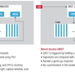
It’s LBIST (Logic Built-in Self-Test) function included in the chip along with a PRPG (Pseudo Random Pattern Generator) and a MISR (Multiple Input Shift Register). All scan elements are provided with known stimuli which are generated by the LBIST macro and are derived from a seed in the PRPG. The static and at-speed testing is done by capturing values and scanning them through the MISR. The MISR contains prior values which are compared with captured values and final MISR signatures are checked to verify the correct operation of the chip.
There are two different types of interfaces to LBIST in the Encounter Test LBISToption to Encounter RC (RTL Compiler). The Direct Access LBIST is easily executed by holding a pin high. The MISR signatures are compared with the stored internal values and a simple go/no-go response is provided to determine if LBIST has finished successfully. The smallest form factor for the Direct Access LBIST macro starts with 100 flip flops. This arrangement is simple and provides high quality results. The other interface, JTAG Access LBIST uses JTAG interface and protocols to start and execute LBIST. The signatures are compared off-chip in a higher level service processor or board-level devices. This arrangement allows customization of LBIST parameters in the silicon to run different testing scenarios. The smallest form factor starts from 160 flip flops. The LBIST macro area is increased to include shorter and more scan channels for increasing the speed of LBIST run.
In order to increase the test coverage, extra testpoints are optimally chosen and placed at suitable locations. This is automatically done by using RRFA (Random Resistance Fault Analysis) technique available in the Encounter Test DFT Architect as an add-on option to Encounter RC. The analysis can be done early in the design cycle to determine if testpoints are needed.
The Encounter RC cockpit provides a seamless environment for insertion and connection of the LBIST macro into the front-end design netlist and optimization of area, power, timing and test coverage through synthesis. The RTL Compiler also generates all downstream scripts to verify design equivalence with Cadence Conformal LEC, generate test patterns, signature, and fault coverage metrics with Encounter Test True Time ATPG, and MISR signature verification with Cadence Incisive ncverilog simulation.
From the safety standard perspective, the automotive industry has set standards such as ISO 26262 and AEC-Q100 which must be met by the hardware and software provided by electronics suppliers. The Cadence Encounter Test LBIST provides an ideal solution to meet these criteria, in-built into the chip and that can be tested throughout the product life cycle.
Although in general LBIST provides a low pin interface, the Direct Access LBIST interface is a unique solution for mixed-signal and pin-limited designs used in automotive applications. Dale Meehl at Cadence has described the overall methodology in a whitepaper posted at Cadence website. It’s an interesting read!
More Articles by Pawan Fangaria…..
lang: en_US