How the Arduino Changed Embedded System Development Forever
In 2005 with the development of the Arduino, everything changed for people building things that required a microcontroller. The Arduino brought with it a low price standard, and open, hardware platform and an easy to use open source development environment. It was not without its limitations, but it opened the doors for literally thousands of people who had ideas and did not want putting together the platform to take most of their time. According to Wikipedia, it is estimated that there are over 700,000 Arduino boards in developer hands.
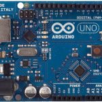
It used to be that you needed to have a hardware programmer and had to master a long complex tool chain to develop, compile, link and load your code. On the hardware side, the Arduino brought a standard form factor and pin-outs, but more importantly standard libraries for things like digital IO, PWM, SPI and I2C. All of this was wrapped in an easy to install and use free development environment based on GNU tools, including a code editor and requiring no command line input. More information and the IDE are available at www.arduino.cc. The programming is made easy to use by simply connecting a USB cable to the board.
Once there was a ‘standard’ many compatible interface boards, called shields, and devices were developed. The libraries for accessing them were openly available in usable source code format for download and reuse. Sensors like MEMS gyroscopes or accelerometers, and proximity, light, temperature, image, touch, etc. became easy to use. Added to this mix were servos, motor controllers, addressable LEDs, and many other devices. Of course hobbyists picked up on this and it became a rapidly growing cottage industry. Just go to retailer sites like www.adafruit.com or www.sparkfun.com to see what is available.
The first Arduino used an Atmel microcontroller from the AVR series. They are 8 bit CPUs running at a modest 8 or 16MHz, digital IOs, and analog inputs. There is also flash storage on-chip for code storage, RAM for program data storage, and EEPROM. Flash and RAM are limited, but enough to get by for small projects. To give you an idea, all the data in your code was typically limited to 2K bytes. But there is no operating system and the program code can be loaded into the flash using a USB cable. The on-chip flash and EEPROM means that these chips were fabricated using older process nodes and proprietary processes.
Despite the initial limitations people became more ambitious with what they built. If you look today at almost any 3D printer or quadcopter, you will see an Arduino hidden inside. Thus the Arduino has become an enabling technology for a new wave of products. One notable example is the OtherMillthat can be used to fabricate custom PCBs at home.
Arduino clones appeared, many of them using the open source schematics from the Arduino Project. This meant that they were compatible with the Arduino IDE, making it easy for people to adopt. Often their code worked without any changes. New form factors were introduced by the Arduino Project, and other new boards appeared from other sources. Even non Arduino boards and non AVR processors could be supported by additions to the Arduino IDE. Today if you go look for Arduino compatible and ‘like’ development boards, you will be confronted by a large array of choices. Large semiconductor companies with their own processors, some of them ARM based, took noticed and developed their own boards and started bringing them the Maker Faire, which draws over 120,000 people in one weekend, in the San Francisco Bay area.
At the recent ARM TechCon, ST was handing out free development STM32L032 boards that use the ARM Cortex M0 core, a low power processor. However this board uses a non-Arduino tool chain, and setting it up requires some effort. This might be fine or someone who wants to develop a Cortex M0 system for a product and does not need the community of knowledge and code that the Arduino has. But the boards are attractively priced and it looks like there are some independent projects to build an Arduino compatible IDE.
Intel has not been absent from this market. They along with ST, Freescale, and others see the potential in this market. This is especially true as these boards gain wireless connectivity, like Bluetooth and even Wifi. Intel has just release a very small form factor board, called Edison, with a 22nm multi core processor using 2 ATOM cores running at 500Mhz. While it is running Yocto Linux, it offers the option of being programmed with the Arduino IDE. Of course you might prefer to write C++ or node.js for the Linux environment, but for getting started the Arduino IDE is hard to beat. This is not their first effort; they have had another board called Galileo out for some time.
But the new Edison board is different. For about $50 it has built in Bluetooth and Wifi, all in an extremely small, but non-standard, form factor. However Intel partnered with one of the well-known Maker retailers, SparkFun.com, to develop carrier boards that do offer the standard Arduino pin-out geometry. It comes with generous code and data space, 4 GB EMMC and 1GB LPDDR3 respectively. Also one of the cores on the die is a 100MHz Quark core that will run an RTOS developed by Intel’s Wind River subsidiary. Presumably serious IoT and wearable product developers will look to this platform as a powerful, low power and compact vehicle for their designs.
We are in the midst of a rapidly growing and changing landscape for small, powerful and easy to integrate and develop for embedded systems. Not even the Arduino Project is standing still. Their first ARM based board was the Due, and used an ATMEL ARM Cortex M3 core. They have already introduced the Yun, which in addition to the traditional 8 bit AVR processor, has an Atheros AR9331 core with an Open-Wrt based Linux along with Wifi to support a REST protocol interface API in the Arduino IDE. And an even newer offering from the Arduino Project has an ATMEL 32 bit ARM Cortex M0+ core to do both the user code execution and manage wireless interfaces. And of course the Arduino IDE can be used for the software development, just like the original 8 bit Arduino boards.