The worldwide TSMC 2025 Technology Symposium recently kicked off with the first event in Santa Clara, California. These events typically focus on TSMC’s process technology and vast ecosystem. These items were certainly a focus for this year’s event as well. But there is now an additional item that shares the spotlight – packaging technology. Thanks to the increase in heterogeneous integration driven in large part by AI, the ability to integrate multiple dies in sophisticated packages has become another primary driver for innovation. So, let’s look at what was shared at the pre briefing by Dr. Kevin Zhang and how TSMC brings packaging center stage with silicon.
A Growing Palette of Options
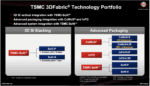
TSMC has taken advanced packaging well beyond the 2.5D interposer approach that is now quite familiar. The diagram above was provided by TSMC to illustrate the elements that comprise the TSMC 3DFabric® technology portfolio. According to TSMC, transistor technology and advanced packaging integration technology go hand-in-hand to provide its customers with a complete product-level solution.
On the left are the options for stacking or die-level/wafer-level integration. SoIC-P ( below) uses microbump technology to deliver down to a 16um pitch. Using bumpless technology (SoIC-X), you can achieve a few micron pitch. TSMC started with 9um and is now in production at 6um with more improvements to come, creating a monolithic-like integration density.
For 2.5/3D integration, there are many options available. Chip on Wafer on Substrate (CoWoS) technology supports both the familiar silicon interposer as well as CoWoS-L, which uses an organic interposer with a local silicon bridge for high-density interconnect. CoWos-R provides a pure organic interposer.
Integrated Fan-Out (InFO) technology began in 2016 for mobile applications. The platform has been expanded to support automotive applications as well.
There is also the newer System-on-Wafer (TSMC-SoW™) packaging. This technology broadens the integration scale to the wafer level. There is a chip-first approach (SoW-P), where the chip is put on the wafer and then an integrated RDL is built to bring the dies together. Or, there is a chip-last approach (SoW-X), where you first build the interposer at the wafer level and then add the chips across the wafer. This last approach can produce a design that is 40X larger than the standard reticle size.
High-performance computing for AI is clearly a major driver for advanced packaging technology. The first diagram below provided by TSMC, illustrates a typical AI accelerator application today that integrates a monolithic SoC with HBM memory stacks through a silicon interposer. Some major improvements that are coming for this type of architecture as shown on the next diagram.
The monolithic SoC is now replaced with a 3D stack of chips to address high-density compute requirements. HBM memory stacks are integrated with an RDL interposer. Integrated silicon photonics will also be part of the design to improve communication bandwidth and power. Integrated voltage regulators will also help to optimize power for this type of application.
Regarding power optimization, future AI accelerators can require thousands of watts of power, creating a huge challenge in terms of power delivery into the package. Integrated voltage regulators will help to tame this class of problem. TSMC has developed a high-density inductor which is a key component required to develop this class of regulator. So, a monolithic PMIC plus this Inductor can provide a 5X power delivery density (vs. PCB level).
There are many exciting new technologies on the horizon which will require all the packaging innovation discussed here. Augmented reality glasses is one example of a new product that will require everything discussed. A device like this will require, among other things, an ultra-low power processor, a high resolution camera for AR sensing, eNVM for code storage, a large main processor for spatial computing, a near-eye display engine, WiFi/Bluethooth for low latency RF, and a digital intensive PMIC for low power charging. This kind of product will set a new bar for complexity and efficiency.
While autonomous vehicles get a lot of attention, the demands of humanoid robots were also discussed. TSMC provided the graphic below to illustrate the significant amount of advanced silicon required. And the ability to integrate all of this into dense, power efficient packages is critical as well.
To Learn More
It was clear at the TSMC Technology Symposium that advanced processing and advanced packaging will need to work as one going forward to achieve the type of product innovation on the horizon. TSMC has clearly taken this challenge and is developing unified offerings to address the coming requirements.
You can learn more about TSMC’s 3DFabric Technology here. And that’s why TSMC brings packaging center stage with silicon.
UPDATE: TSMC is sharing recordings of the presentations HERE.
Also Read:
TSMC 2025 Technical Symposium Briefing
IEDM 2025 – TSMC 2nm Process Disclosure – How Does it Measure Up?
TSMC Unveils the World’s Most Advanced Logic Technology at IEDM
IEDM Opens with a Big Picture Keynote from TSMC’s Yuh-Jier Mii