Design & Reuse recently held its IP-SoC Days event at the Hyatt Regency in Santa Clara. Advanced IP is now the fuel for a great deal of innovation in semiconductor design. This popular event allows IP providers to highlight the latest products and services and share a vision of the future. IP consumers can easily get updates on the latest IP technology trends and innovations all at one event. There was a presentation that dove into a lot of very relevant details. The information was complete and compelling. In case you missed the event, here is a summary of how Silicon Creations presents architectures and IP for SoC clocking.
About the Authors
The presentation was given by Jeff Galloway, co-founder of Silicon Creations. Jeff has a long career in analog/mixed signal design dating back to Hewlett Packard in the late 1990’s. He also developed advanced AMS designs at Agilent and MOSAID/Virtual Silicon before founding Silicon Creations in 2006. His command of the challenges of AMS design and the impact these designs have on innovation is substantial. Jeff brought a lot of perspective and insight to the presentation.
The paper was co-authored by Krzysztof Kasiński, Director of IP Validation Laboratory at Silicon Creations and University Professor at AGH University of Kraków.
About Silicon Creations
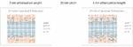
Silicon Creations is a self-funded, leading silicon IP provider with offices in the US and Poland as shown in the diagram above. The company has sales representation worldwide and delivers precision and general-purpose timing (PLLs), oscillators, low-power, high-performance multi-protocol and targeted SerDes and high-speed differential I/Os. This IP is used in diverse applications including smart phones, wearables, consumer devices, processors, network devices, automotive, IoT, and medical devices. An overview of where you will find Silicon Creations IP is also shown in the diagram above.
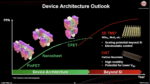
The company works with many foundries, delivering IP in planar, FinFET, FD-SOI, and Gate-All-Around technologies. The company reports that the majority of the world’s top 50 IC companies are working with Silicon Creations. The figure below shows the substantial ecosystem footprint the company delivers.
Problems to be Solved
Clock jitter provides a lot of headaches for advanced design teams. This is the situation where clock edges move from the ideal locations. Clocking systems should be designed with jitter in mind to avoid system level problems.
The diagram above, provided by Silicon Creations, provides some context for the jitter types by application. It turns out various applications require different clock quality metrics. Here are some examples:
- Generic, digital synchronous logic: Total period jitter (peak-negative) to define clock uncertainty for STA
- Multi-cycle paths and e.g. DDR controllers: N-period jitter (depending on number of cycles / latency)
- ADC/DAC: Long-term jitter / Phase Noise to achieve ENOB; LJT reduces ENOB
- RF: Long-term jitter / Phase Noise to low Error Vector Magnitude; LTJ rotates constellation increasing EVM
- SerDes: Clock specification (including integration bands) tightly related to the protocol and PHY vendor. Possible filtering (e.g. PCIe spec). Embedded clock applications require low LJT
Jitter can come from many sources. Here are some examples provided by Silicon Creations with the type of remediation required:
- FREF signal quality including impact from its signal path à design choices
- PLL design and operating point (FPFD, FVCO, FOUT configuration, PVT condition) à IP vendor + programming
- PLL conditions (decoupling, supply noise) à IP vendor support + design choices
- Output clock path (supply noise, length / delay, additive jitter) à design choices
The Silicon Creations Approach
Jeff provided a very informative chart (below) that shows where the company’s broad IP portfolio fits in advanced designs.
It turns out a large library of precision IP is needed to address clocking challenges in advanced designs. Silicon Creations has developed a comprehensive approach to these challenges. The chart below provides an overview of the various types of designs requiring help and how the Silicon Creations IP portfolio fits.
In his presentation at IP-SoC Days, Jeff provided examples of how Silicon Creations IP provides design teams options for dealing with clocking issues. He also provided an informative chart of a PLL performance matrix for its IP across frequency, area, and power. It turns out Silicon Creations PLL IP covers a vast range of performance metrics and can be a fit to many applications. Here are some highlights:
- Power: below 50 µW through 5mW up to 50mW
- Area:07mm2 through 0.1mm2 up to 0.14mm2
- Output Frequency Range: From MHz range up to tens of GHz; frequency jumping, glitch-free operation, de-skewing
- Reference Frequency Range: From 32kHz, through all crystal oscillator types, external clock chips, on-chip de-skewing
Jeff also described the comprehensive engagement process the company offers its customers. He explained that the Silicon Creations engineering team is involved from the beginning to help design SoC clock systems, from IP through distribution to the power delivery network. An overview of the engagement process is provided below.
To Learn More
If you are doing advanced designs that are performance sensitive, you will likely face the kind of clocking problems that Silicon Creations can address. The company’s broad, high-quality IP portfolio and domain expertise can be a real asset.
You can access the Silicon Creations presentation from IP-SoC days here. And you can preview Silicon Creations’ IP portfolio on Design & Reuse here.
Of course, you can also learn more about Silicon Creations at the company’s website here. There is also some excellent in-depth coverage on SemiWiki here. And you can always reach out to the company to start a dialogue here. And that’s how Silicon Creations presents architectures and IP for SoC clocking at IP-SoC Days.