webinar IPXACT banner

Simulating Full-System EMI for a Car in Just 28 Minutes

Simulating Full-System EMI for a Car in Just 28 Minutes
by Bernard Murphy on 10-23-2015 at 8:00 pm

While there’s a lot of cool technology in modern semiconductors, it’s important to raise our sights periodically to understand how well these chips will work in the systems for which they are designed. One area driving a lot of semiconductor growth is automobile electronics. We’ve had drive-train control forever it seems, but now that is enhanced to provide user-selectable ride-control. More recently we have seen advanced driver assistance systems, high-end infotainment options, mobile hot-spots, Bluetooth-enabled links to smart phones and more. But all that fancy electronics won’t be very useful (and might well become dangerous) if disrupted by external and internal EM interference. One big concern is the antenna represented by as much as 5 kilometers of interconnect in modern cars, which can both receive and transmit EM. Multiple radio sources from phones, tablets and Bluetooth devices inside or outside the car add to EMI concerns.

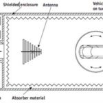
Amazingly (ha-ha) there are standards for automobile electronics beyond ISO 26262. ISO 11451-2 defines expectations for minimum EMI immunity in vehicle electronics. This requires measurements in and around the complete vehicle in an anechoic chamber. An antenna in the chamber generates RF waves swept by strength and frequency over specified ranges and interference is monitored at select test points in the car. Final testing must follow this methodology, but it is an expensive approach to require for experimentation during the design phase.

As always, simulation is the optimum approach for design but this is complex analysis problem. You have to model electronics and cabling, the car frame and the EM sources. ANSYS® pioneered in their HFSS software a Finite Element Method (FEM) simulation approach called the “domain decomposition method” (DDM) which makes it possible to parallelize the analysis across multiple machines. This itself was a big step forward in making numerical simulation a practical alternative to chamber testing.

For those of you who don’t know this domain so well, HFSS is the industry standard for full-wave electromagnetic field simulation. It is used extensively for design of antennas, communications systems, radar systems, satellites, smart phones and tablets and transportation electronics. It also integrates with ANSYS multiphysics solutions so you can, for example, combine electromagnetics simulations with thermal simulations.

ANSYS recently introduced a refinement to HFSS called FE-BI, using an integral equation approach to truncate boundaries around EM emitters and around the car; this greatly reduces the space that must be considered in analysis while preserving the accuracy of a complete FEM analysis. The impact of that reduction in a joint test with Fiat-Chrysler was a 10-fold increase in performance and a 10-fold reduction in memory demand. A realistic simulation of an external antenna transmitting from a distance to a car frame completed in just 28 minutes and calculated electric fields matched closely with a full FEM analysis.

Full-space FEM simulation
Reduced space determined by the BI method
Reduced-space simulation closely matching the full-space simulation

Fiat-Chrysler engineers were also able to model the effect of a wiring harness as a transmitter inside the car, allowing them to determine the effects of coupling between the harness and a connected PCB. What impresses me about all of this analysis is the scale and detail it comprehends – from PCBs and individual wire connections, through the full car-frame, to external EM sources some distance away from the car. To design for the complexity we demand today in auto electronics and yet still to be able to model EMI to a level allowing detailed design decisions to optimize immunity, this is a high order of modeling.

To lean more about HFSS-BI and the Fiat-Chrysler experiments, click HERE.


More articles by Bernard…


ARM Keil Ecosystem Integrates Atmel SAM ESV7

ARM Keil Ecosystem Integrates Atmel SAM ESV7
by Eric Esteve on 10-23-2015 at 4:00 pm

Even the best System-on-Chip is useless without software, as well as the best designed S/W needs H/W to flourish. The “old” embedded world has exploded into many emergent markets like IoT, wearable, and automotive is no more restricted to motor control or airbags as innovative products, from entertainment to ADAS are being developed. What is the common denominator with these emergent products? All of these are requiring more software functionality and fast memory algorithm with deterministic code execution and consequently innovative hardware supporting these requirements, like ARM Cortex-M7 based Atmel SAM ESV7.

ARM has released a complete software development environment for a wide range of ARM Cortex-M based microcontroller devices, Keil MDK. Keil is part of ARM wide ecosystem, allowing developers to speed up system release to the market. MDK includes the µVision IDE/Debugger, ARM C/C++ Compiler, and essential middleware components and software packs. If you are familiar with Run-Time Environment stacked description, you can recognize the various stacks. Let’s focus on “CMSIS-Driver”. CMSIS is the standard software framework for Cortex-M microcontrollers, extending the SAM-ESV7 Chip Library with standardized drivers for middleware and generic component interfaces.

By definition, MCU is designed to address multiple applications and Atmel SAM ESV7 is dedicated to support performance demanding and DSP intensive systems. Thanks to the 300 MHz clock, SAM ESV7 delivers up to 640 DMIPS and its DSP performance is double that available in the Cortex-M4. A double-precision floating-point unit and a double-issue instruction pipeline further position the Cortex-M7 for speed.


Let’s review some of these applications where SAM ESV7 is the best choice.

Finger Printer Module

The goal is to provide human bio authentication module for office or house access control. The key design requirements are:

  • +300 MHz CPU performance to process recognition algorithms.
  • Image Sensor Interface to read raw finger image data from finger sensor array.
  • Low cost and smaller module size: Inside Flash/Memory to reduce BOM cost and module size.
  • Memory Interface to expand model with memory extension just in case.

The performance requirement and the need for Image sensor Interface can be seen as essential needs, but which will make the difference will be to offer both cheaper BOM cost and smaller module size than competitor. The SAM S70 integrates up to 2 MB embedded Flash, which is twice more than the direct competitor and may allow reducing BOM and module size.

Automotive Radio System

Each $ cent count in automotive and OEM prefer using a MCU than MPU, at first for cost reason. Building an attractive radio for tomorrow’ car require developing very performing DSP algorithms. Such algorithms used to be developed on expansive DSP standard part, leading to large module size, including external Flash and MCU leading obviously to a heavy BOM. In a 65nm embedded Flash process device, the Cortex-M7 can achieve a 1500 CoreMark score while running at 300 MHz, and its DSP performance is double that available in the Cortex-M4. This DSP power can be used to manage 8 channels of speaker processing, including 6 stages of Biquads, delay, scaler, limiter and mute functions. Atmel SAM S71 workload is only 63% of the CPU, leaving enough room to support Ethernet AVB stack, very popular in automotive.

One of the secret sauces of the Cortex-M7 architecture is to provide a way to bypass the standard execution mechanism using “tightly coupled memories,” or TCM. There is an excellent white paper describing TCM implementation in ARM Cortex-M based Atmel SAM S70/E70 series, “Run Blazingly Fast Algorithms with Cortex-M7 Tightly Coupled Memories” from Lionel Perdigon and Jacko Wilbrink, that you can find here.

More about Keil MDK

Getting started with Atmel SAM V7 Video

From Eric Esteve from IPNEST


Three New Things from ITC this year

Three New Things from ITC this year
by Daniel Payne on 10-23-2015 at 12:00 pm

The NFL has its annual Super Bowl contest each year, EDA vendors attend DAC, then the test folks attend ITCwhich was in Anaheim a few weeks ago. I’ve marketed ATGP, BIST and DFT tools before so I like to keep updated on what’s happening at conferences like ITC. Robert Ruiz from Synopsys spoke with me by phone to provide an update on three new things that they shared at ITC this year.

  • New ATPG Technology
  • ISO 26262-5 Certification (Auto reliability standard)
  • Improved support of FinFET and emerging node tests

New ATPG Technology
You can only enhance EDA software so much by adding incremental new features, sometimes you have to start over from scratch in order to achieve something great, and in this case the engineers at Synopsys did a re-write of their ATPG algorithm in order to produce new results that complete some 10X faster than before. Just think about that, having to wait either 10 hours or just 1 hour. Of course, we all want that 1 hour result because of the productivity gains provided.

This faster ATPG engine takes more effective advantage of all cores in your machine. In the previous ATPG algorithm each core would read in the entire design, while with the new algorithm the paths for each fault are distributed to an available core, thus using far less RAM. Here’s a look at some actual ATPG runt time speed up results across five different designs:

Your time spent to diagnose where faults are located in actual silicon are also sped up now. This improvement helps foundries and IDMs to bring up new process nodes quicker.

Another benefit of the new ATPG engine is that the quality of the patterns has improved, so you can expect a reduction in the number of test patterns by around 25% as shown below:

ISO 26262-5

The automotive market is adopting an increasing amount of semiconductor content with each new generation of vehicles, and this market has a well-defined requirement for functional safety as defined by the ISO 26262 certification standard. The actual design process and EDA software must meet the ISO standards. To that end, the following Synopsys EDA tools have achieved this functional safety certification process:

  • TetraMAX ATPG
  • DFTMAX Ultra
  • DesignWare STAR Memory System
  • STAR Hierarchical System

FinFET and Emerge Node Tests

With FinFET transistors there are new process defects that require new fault models like:

  • Metal shorts
  • Open vias
  • Resistive shorts
  • Resistive opens
  • Litho induced defects

You really need cell-aware faults based upon transistor-level defects found inside of the cells.

You can now perform cell-aware characterization using a SPICE tool like HSPICE in about one day, which is another 10X speed improvement.

Summary

The faster, more efficient ATPG algorithms at Synopsys are certainly going to make test engineers more productive in their jobs. Complying to the ISO standard for automotive safety will be another benefit of using the Synopsys DFT tools. Finally, you can be confident on FinFET designs that the silicon defects are properly modeled.

The big question is, when I get a hold of this new technology? Early customers should get the first use of this technology by the end of the year.

Related Blogs


Why FPGA synthesis with Synplify is now faster

Why FPGA synthesis with Synplify is now faster
by Don Dingee on 10-23-2015 at 7:00 am

The headline of the latest Synopsys press release drops quite a tease: the newest release of Synplify delivers up to 3x faster runtime performance in FPGA synthesis. In our briefing for this post, we uncovered the surprising reason why – and it’s not found in their press release. Continue reading “Why FPGA synthesis with Synplify is now faster”


FinFET Reliability Analysis with Device Self-Heating

FinFET Reliability Analysis with Device Self-Heating
by Tom Dillinger on 10-22-2015 at 12:00 pm

At the recent TSMC OIP symposium, a collaborative presentation by Synopsys and Xilinx highlighted the importance of incorporating the local FinFET device self-heating temperature increase on the acceleration of device reliability mechanisms.
Continue reading “FinFET Reliability Analysis with Device Self-Heating”


How Virtualization Makes Network Processor Verification Efficient

How Virtualization Makes Network Processor Verification Efficient
by Tom Simon on 10-22-2015 at 7:00 am

When Ethernet was introduced in 1983 it ran at 10Mbps and mostly relied on hubs and coaxial cable. Twelve years later a faster speed was introduced, running at 100Mbps. Since then we have seen an acceleration of new data rate introductions. According top the Ethernet Alliance, Ethernet could have 12 speeds before 2020, with 6 of those new speeds introduces in the next 5 years.

At the high-end, 25G, 50G and 100G data rates are necessary for supporting the massive growth of internet traffic. The first networks in the 80’s used hubs with very simple circuits and 10’s of ports. Today’s routers and switches have sophisticated network processors that provide numerous services to maintain throughput and manage traffic. The complexity of networking chips is second only to CPU and GPU chips. The number of ports is driving up beyond 256 heading toward 1024.

I find it fascinating that the compute power of the network itself often exceeds the compute power of the things we are connecting to it. The number of gates required is well into the hundreds of millions. With the increasing complexity of network processors comes a need for increasing verification performance. HDL simulators can run at effective speeds of ~100Hz. That translates into only 1,000 packets per day, which is not enough to permit adequate functional verification prior to tape out. The cost of a missed bug is potentially millions of dollars.

In circuit emulation (ICE) in a verification lab has been the fallback for many companies to achieve better verification. However, this still is not an ideal solution. Huge rat’s nests of cables are required. An engineer often needs to be physically present to set up, fix cables and run tests. Unfortunately, the need to run tests with the system software running on the system hardware remains as critical as ever.

Taking a page from the virtualization trend seen in data centers, Mentor Graphics decided to implement what they call a VirtuaLab for verifying next generation protocols in a tractable fashion. The key to this is using their Veloce hardware emulator to accelerate simulation speed to be able to simulate over 11 million packets per day. Veloce offers visibility and traceability that is not available in ICE approaches. This means that when bugs are found, they are more easily tracked down.

The traditional deal breaker for emulation is capacity. To solve this problem Mentor took the approach of designing their own ASIC, called Crystal 2, for their emulator. Higher capacity per chassis means a cleaner set up in the data center. Their largest configuration supports running designs with 2 billion gates. No tangles of wires connecting boxes are needed. The Ethernet testers can run on a regular workstation and can drive many ports per workstation.

The VirtuaLab is not new, but Mentor just announced support for the latest and highest speed Ethernet specifications, 25G, 50G and 100G. They also provided a lot of customer testimonial information to illustrate the efficacy of the Veloce emulation solution for network chip design.

I had a chance to listen to Jean-Marie Brunet, Marketing Director for the Emulation Division at Mentor Graphics discuss the new features in Veloce VirtuaLab. During the presentation he discussed two compelling case studies. The first was Juniper Networks using Veloce to verify a network switch with multiple 10G ports. They were streaming 64-byte packets. They were able to run billions of transactions of 64 bytes up to jumbo across all ports. They went from ¼ frame per second with simulation to ~3,662 frames per second with Veloce. The second case study features Cavium. They were able to go from 1,000 packets per day up to 11 million by switching to Veloce.

Mentor continues to show its prowess in the emulation arena. It’s good to see how emulation can be used to dramatically improve pre-silicon verification of complex hardware-software systems.


Interconnect Watch: 3 Chip Design Merits for Network Applications

Interconnect Watch: 3 Chip Design Merits for Network Applications
by Majeed Ahmad on 10-21-2015 at 4:00 pm

The countdown to the end of Moore’s Law is coinciding with the rising complexity in system-on-chip (SoC) designs. And that’s not a mere coincidence. The leverage that has long been coming from shrinking process nodes in terms of cost, performance and power benefits is now increasingly being accomplished through greater efficiency in SoC designs.

Take, for instance, interconnect, one of the few configurable venues left on the SoC real-estate. So far, internal chip design teams have been relying on legacy interconnect technologies such as hierarchical bus and configurable crossbar. However, cost imperatives, time-to-market pressure, and design challenges like routing congestion and place-and-route issues are forcing SoC designers to consider the interconnect IP implementations.

Montage Technology, a chip supplier for home entertainment and cloud computing markets, has licensed Arteris FlexNoC IP for its digital set-top box (STB) chipsets. Arteris’ network-on-chip (NoC) technology alleviates bottlenecks in moving large blocks of data by packetizing data and serializing transmission over fewer wires than required in other interconnect technologies.


Interconnect architecture for an STB chipset

The market for STB-like devices is essentially flat, but the technology content inside them is increasing. For markets like China, the over-the-top (OTT) STB and other media server devices have the opportunity to become the hub, where a number of home entertainment and consumer electronics devices can be connected.

Next, two of the world’s largest enterprise SSD manufacturers have licensed Arteris FlexNoC interconnect IP for use as the communications backbone in their SSD controller chipsets. So what makes interconnect IP solutions like Arteris FlexNoC appealing for network-centric chipset designs?

The blog takes a peek at three design venues that particularly suit SoCs for moving large blocks of data very quickly.

Bandwidth and Latency Management

The bandwidth and latency features are intrinsically linked to network communications, and both of these features come under the requirement commonly known as Quality-of-Service or QoS. The latency- and bandwidth-related QoS requirements often conflict in a complex system, and to address these conflicts, Arteris’ on-chip interconnect technology implements cascaded arbitration throughout the NoC framework.

Arbiters at each switch make a cascade that is needed for timing closure. That allows simpler and lightweight logic, which in turn, leads to less area, lower cost and power savings. Master starvation and head-of-line (HOL) blocking performance limitations common in data networks are addressed by communication between arbiters that allow for Pressure and Hurry.


Communication between arbiters for managing heterogeneous traffic

Pressure pushes a pending transaction that is blocking a higher priority transaction. Hurry forces a response to return as soon as possible. The end-to-end QoS—from initiator/master to target/slave—and data traffic arbitration features offered by the Arteris FlexNoC interconnect fabric can play an important role in facilitating high-bandwidth video streams and low-latency on-chip communications.

Memory Efficiency

For home entertainment products like OTT STB, contention for memory is of extreme importance because of the mix of one or more decoded video streams as well as audio and overlays. That makes efficient DRAM utilization a key requirement in optimal system-wide performance.

Arteris FlexNoC’s FlexMem memory scheduler ensures that transactions are ordered properly to meet the QoS requirements dictated by the user. Moreover, it ensures that the memory controller does not unnecessarily reorder these transactions.

The memory scheduler logic understands the QoS scheme and sends data to the protocol controller to ensure that system-wide QoS is met; not just memory utilization and efficiency goals in isolation.

The Arteris FlexNoC memory scheduler also implements reorder buffering to accommodate LPDDR4 per-bank refresh. All-bank refresh means the whole die is locked out during refresh, while in per-bank refresh, one bank is locked out at a time during refresh but other seven banks are available. Here, memory scheduler indicates when to refresh and which banks.

On-chip Data Security

Security is a growing concern in the next-generation networking environments like the Internet of Things (IoT). Case in point: SSD controller SoCs must protect data contents not only within processing units and memories but also in on-chip communications between them.

Arteris FlexNoC interconnect IP features ECC and parity data protection that make it easy to set up, test and check the composition of on-chip data flows in real-time. Moreover, FlexNoC fabric natively supports the ARM Cortex-R5 and Cortex-R7 processor ECC and parity data protection schemes.


FlexNoC Resilience Package is developed for safety-related SoC designs in the automotive, industrial and medical markets

Next, Arteris makes available data security features such as redundancy, duplication and built-in system test (BIST) with the optional FlexNoC Resilience Package.

Also read:

SSD Storage Chips: Basic Interconnect Considerations

Is Interconnect Ready for Post-mobile SoCs?

Rockchip Bets on Arteris FlexNoC Interconnect IP to Leapfrog SoC Design


The best possible merger in the Semiconductor Capital Equipment Business history!

The best possible merger in the Semiconductor Capital Equipment Business history!
by Robert Maire on 10-21-2015 at 12:00 pm

A new powerhouse to dominate over AMAT
Combination of best of Breeds
KLAC shareholders get $32 cash plus stock


The wedding invitation…….

Lam Research Corporation (NASDAQ: LRCX) (“Lam”) and KLA-Tencor Corporation (NASDAQ: KLAC) (“KLA-Tencor”) today announced that they have entered into a definitive agreement, unanimously approved by the boards of directors of both companies, for Lam Research to acquire all outstanding KLA-Tencor shares in a cash and stock transaction.

KLA-Tencor stockholders will be entitled to elect to receive for the shares of KLA-Tencor stock they hold the economic equivalent of $32.00 in cash and 0.5 of a share of Lam Research common stock, in all-cash, all-stock, or mixed consideration, subject to proration as more fully described in the merger agreement. The transaction values KLA-Tencor at approximately $67.02 per share, or $10.6 billion in equity value based on the closing stock price of Lam on October 20, 2015.

This combination will create unmatched capability in process and process control, delivering optimized results in partnership with its customers by reducing variability and accelerating yield, ultimately helping the semiconductor industry extend Moore’s Law and performance scaling generally.
The combined company will have approximately $8.7 billion in pro forma annual revenue

Full press release of merger
There will be a conference call at 5AM PST

Both a powerhouse and a dream team in SemiCap…
Much as the merger between Lam and Novellus seemed to be talked about for quite some time before it finally happened so too has the combination of Lam and KLA been the subject of speculation especially after the announced merger of AMAT and TEL would seem to have forced the reaction from both companies. Now the combination is announced without the threat of the AMAT merger and puts the resulting Lam into a very dominant position. We think there is a clear strategic benefit of putting process control together with a process company as we get to ever smaller and difficult dimensions of Moore’s law.

A torpedo in the side of AMAT…
After reeling from the failed merger with TEL and trying to regain its momentum and composure , Applied Materials has just been hit with a merger that will leave it in second place., dazed and confused. The combined LAM and KLA creates a powerhouse in the semicap industry which is looking a lot more like a duopoly (without litho…)

We told you so…..
Way back in April of 2014 we both predicted the combination and talked about the company’s new lead product.

Recently merged KLAM’s first new product..
The recently merged combination of KLA and Lam (ticker KLAM) introduced its first product as a joint company the “Characteristic Highlighting On Wafer Defect Analyzer” (CHOWDA). A spokeswoman for the company, Sharee Lewis said ” The new KLAM CHOWDA product will be available in two implementations to account for regional technical differences. Introduction of the product will start in the summer”.

The Stocks…
This is obviously a no brainer, huge positive for LAM and a huge negative for Applied. Likely a negative for smaller process control and metrology companies as they become less relevant.

Adds to the $100B in announced Semiconductor deals…
Spring is in the air and the urge to merge clearly continues to be very very strong especially as valuations remain low and attractive.

Will the deal get through?
We think this is going to be the obvious biggest issue after the failed AMAT & TEL merger. We think there will likely be opposition in the semi industry but probably less so than we heard the screaming related to AMAT/TEL. While maybe not overjoyed , the combination makes a lot of sense for customers and feels a lot less negative than the failed AMT/TEL

We will have a lot more after the conference call…

Robert Maire
Semiconductor Advisors LLC


Innovative Apps to Evolutionize Wearable Segment

Innovative Apps to Evolutionize Wearable Segment
by Pawan Fangaria on 10-21-2015 at 7:00 am

In recent years, excessive cold or heat in particular regions of the world has become a regular phenomenon; it reminds me about a movie I saw a couple of years ago, “The Day After Tomorrow” in which the whole Manhattan was shown covered with ice. Can’t say whether that can ever happen if at all, but on a better note today, I can see the possibility of our (may be our children’s if not ours) average lifespan increasing to more than 100 years. Well, there are many initiatives going into this longevity drive, ‘Google X’ research being one among other researches on DNA, Stem Cells and so on. I, being a semiconductor professional, am particularly envisioning how semiconductors would influence the human life.

In March, I had written an article on rising medical semiconductor market which was based on semiconductor IC usage in the medical devices along with the data from an IC Insights’ report. Also there are reports from different research agencies on how wearable segment will influence the overall semiconductor market in next five years. Wearable devices are the most appropriate for collecting data from human body for various diagnostic purposes. The data can be used to take preventive measures, thus increasing life expectancy. Medical applications are expected to boost the wearable segment in major way.

Today we are seeing most of the consumer electronic vendors launching their versions of smartwatches, also prompting the traditional watch vendors to launch theirs. However, most of the smartwatches have more or less similar features, either focused on tech quotient or on fashion; of course there are usual heart monitoring, sports, and health tracking apps. There is very less emphasis on specific and unique value a consumer can or should get out of her smartwatch. There is no doubt, the smartwatch is a very powerful device electronically and can do many things, but it needs creative thinking by marketers to work on those. That’s where the software comes into picture, but the app writers alone cannot do the job of creating specialized apps. For healthcare and medical apps, doctors and medical practitioners are required to infuse that knowledge, and then statistics from sample respondents because an app has to determine something out of some symptoms based on the intelligence it has stored from the data of those respondents.

It’s a long drawn process to evolutionize healthcare through wearable semiconductor devices in this way, but the process has begun. I was particularly intrigued after knowing about the Apple ResearchKit which is being populated with several information including data, tasks, methods, and so on by qualified medical practitioners and researchers as well as participants who have consented to provide anonymous data. The ResearchKit study apps are available on Apple’s app store; new apps are being added gradually. It’s interesting to learn that these apps, after their completion, are bound to be cleared by US FDA for mainstream use as medical apps.


Recently a ResearchKit study was done at John Hopkins University for detection of epilepsy. The epileptic seizures are unpredictable, can occur at any time in any condition the human being is. This app is being named as “EpiWatch”. In this study, the Apple Watch sensors are being used to collect the data from human body that help in tracking and sensing seizures. The accelerometer and gyroscope in the watch can help track the movements involved in the seizures. In seizures without any movement, the change in person’s heart rate is detected. The app collects the sensor data along with information from surveys filled out by the participants to study duration, frequency, and type of seizures.

Also there are other research studies being done involving ResearchKit and iPhone as well; ‘Autism and Beyond’ at Duke University, ‘Mole Mapper’ at Oregon Health and Sciences University, and some more. You can see a detailed report about these studies HERE.

I like Apple’s indulgence in experimenting new possibilities with their devices. Developing such apps on smartwatch can definitely add unique value to establish the “smartwatch” as a separate brand irrespective of what traditional watches do. This provides a great clue to the questions on how smartwatch market should evolve in one of my earlier articles – “Smartwatch – A Tough Puzzle to Crack”.

Although Apple Watch, just after its 1[SUP]st[/SUP] launch, is second in wearable market share, it didn’t get the response as was expected. However, once various kinds of medical apps on smartwatch become a reality for mainstream use, it will establish a new market for smartwatches. Apple can definitely be the leader, but it will open up the market for other smartwatch makers as well.

My article based on medical semiconductor market – Medicals Marriage with Semis.