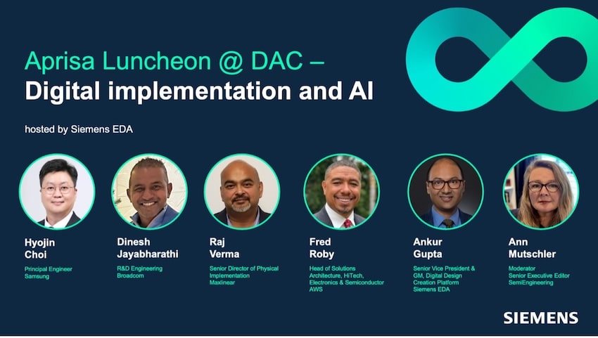
Banner 800x100 0810

Analog Bits Builds a Road to the Future at TSMC OIP

Analog Bits Builds a Road to the Future at TSMC OIP
by Mike Gianfagna on 10-21-2024 at 6:00 am

Analog Bits Builds a Road to the Future at TSMC OIP

The TSMC Open Innovation Platform (OIP) Ecosystem Forum has become the industry benchmark when it comes to showcasing industry-wide collaboration. The extreme design, integration and packaging demands presented by multi-die, chiplet-based design have raised the bar in terms of required collaboration across the entire supply chain. World-class development and collaboration were on display at the recent event, which was held in Santa Clara on September 25, 2024. A critical technology required for success is enabling IP, in particular for sensing and power management.  Analog Bits showcased substantial capabilities here. Let’s examine some of the work presented to see how Analog Bits builds a road to the future at TSMC OIP.

IP Development Progress

Analog Bits discussed some of the unique challenges advanced chip and multi-die design presents. Multi-domain sensing was discussed, along with the additional challenge of non-uniform thermal distributions. Real-time monitoring is another requirement. If the face of all this, calibration complexity, voltage supply noise, and crosstalk must all be dealt with as well.

Analog Bits portfolio of on-die sensing IP was presented, including:

  • PVT Sensors – integrated and pinless
  • Power on reset and over current detection macros
  • Power supply detectors that include:
    • Fast detecting glitch
    • Synchronized droop detection with filtering and differential sensing

The benefits of a comprehensive on-die sensing IP portfolio were also discussed. At the top of the list is improved power efficiency. A good approach here also prevents overheating and minimizes thermal stress. The overall benefits of enhanced reliability and improved yield also come into play.

Power management is also a key benefit. Things like voltage scalability, voltage spike, and droop protection are examples. Better integration that results in space savings is an added benefit.

Analog Bits presented a significant amount of silicon data based on a TSMC N3P test chip. The graphic at the stop of this post is an overview of what’s on this chip. There were many impressive results to show. Here is a list of some of them:

  • Temperature linearity and precision for the High-Accuracy Thermometer
  • Linearity and precision for the high-accuracy Voltage Sensor
  • Measured trigger voltage vs. threshold and untrimmed threshold accuracy for the Droop Detector
  • An overview of Low-Dropout (LDO) regulator development

Regarding the LDO, here is a summary of the program:

  • First LDO modules proven in silicon
  • Latest N3 test-chip taped out Q2 2024
  • Packaging and initial bring up Q1 2025
  • Automotive planned for mid-2025

Here is an example of the data presented. The plot is showing Voltage Sensor accuracy with the following parameters: VDDA: 1.2V, VDD: 0.75V, Corner: TT.

Voltage Sensor Accuracy

IP Collaboration Progress

OIP is all about ecosystem collaboration, so Analog Bits teamed with Arm to present an impressive presentation entitled, Optimized Power Management of Arm CPU Cores with Integrated Analog Bits Power Management and Clocking IP’s. The presenters were Lisa Minwell, Director of Technology Management at Arm and Alan Rogers, President at Analog Bits.

The once-in-a-generation transformation occurring in digital infrastructure was discussed. Complexity increases in data center SoC’s, coupled with AI deployment has made energy efficiency a central issue. It was pointed out that advanced chip and chiplet-based designs in 3nm and 2nm are integrating many Arm Neoverse cores.

The need for managing power to these cores on a granular level is getting increasingly important. The traditional methods of using off-chip LDO and power sensors no longer scales.  A new approach is needed.

The work Analog Bits and Arm have done on several integrated power management and clocking IPs was presented. Arm customers can readily use these solutions in N3P and soon in N2P. LDO regulator IPs were also discussed to efficiently manage the large absolute and dynamic current supplies to Arm CPU cores.

A case study of how CPU cores seamlessly integrate with Analog Bits LDO and Power Glitch Detector IPs, along with integrated clocking capabilities was also presented.  The implications of this work is substantial for advanced data center applications.

To Learn More

I have presented some of the highlights of Analog Bits presence at TSMC OIP. There is a lot more to the story, and you find out more about Analog Bits industry impact on SemiWiki here. You can also check out the company’s website here. And that’s how Analog Bits builds a road to the future at TSMC OIP.


Podcast EP254: How Genealogy Correlation Can Uncover New Design Insights and improvements with yieldHUB’s Kevin Robinson

Podcast EP254: How Genealogy Correlation Can Uncover New Design Insights and improvements with yieldHUB’s Kevin Robinson
by Daniel Nenni on 10-18-2024 at 10:00 am

Dan is joined by Kevin Robinson, yieldHUB’s Vice President of operations and sales. With over 23 years of experience as a test engineer in the semiconductor industry, Kevin brings a wealth of knowledge and dedication to his dual role. At yieldHUB, Kevin leads both sales and operations teams, playing a crucial role in delivering top-notch experiences to UK and European customers.

In this informative discussion, Dan explores with Kevin what genealogy correlation is and how this technique can be used to analyze and optimize yield and performance. By comparing and correlating observed data with expected results based on fab parameters, complex and subtle relationships can be found.

These relationships may not be clear at first, but after applying complex correlation analysis to massive data sets with yieldHib’s automated technology, new relationships between the process, the design, and associated design sensitivities can be quickly uncovered that can have a significant impact on overall yield and performance.

The views, thoughts, and opinions expressed in these podcasts belong solely to the speaker, and not to the speaker’s employer, organization, committee or any other group or individual.


CEO Interview: Dr. Mehdi Asghari of SiLC Technologies

CEO Interview: Dr. Mehdi Asghari of SiLC Technologies
by Daniel Nenni on 10-18-2024 at 6:00 am

Dr. Mehdi Asghari

Mehdi is a serial entrepreneur with a track record of success. He is currently CEO and co-founder of SiLC. SiLC is his third Silicon Photonics start up focusing on advanced imaging solutions that enable machines to see like humans. His previous start up, Kotura where he was CTO and SVP of Engineering, developed communication solutions for data center applications. Kotura was acquired by Mellanox in 2013 where Mehdi continued to serve as VP of Silicon Photonics for over 4 years. Prior to that Mehdi was the VP of R&D at Bookham, the first company to ever commercialize silicon photonics. Bookham focused on sensing and telecom applications and had a successful IP in 2000 with a valuation of ~$7B.

Mehdi is one of the early pioneers of silicon photonics industry with over 25 years of commercialization experience in this space. Prior to that he spent 10 years in the III/V industry.

Tell us about your company.

On a mission to enable machines to see like humans, SiLC Technologies is a silicon photonics innovator delivering coherent vision and chip scale FMCW LiDAR solutions. SiLC has developed the industry’s first fully integrated coherent LiDAR chip. Our breakthrough 4D+ Eyeonic Chip integrates all photonics functions needed to enable a coherent vision sensor, offering a tiny footprint while addressing the need for low cost and low power. SiLC’s innovations are targeted to robotics, mobility, perimeter security, industrial automation and other leading markets. SiLC was founded in 2018 by silicon photonics industry veterans with decades of commercial product development and manufacturing experience.

What problems are you solving?

AI is all the rage now, but its scope to date is limited to the non-physical world. As the author Joanna Maciejewska said, “I want AI to do my laundry and dishes so that I can do art and writing, not for AI to do my art and writing so that I can do my laundry and dishes.” Beyond the desire for more creative and recreational time, the continued economic growth of industrialized countries depends on addressing the severe labor force shortage caused by the persistent (~1% per year) decline in the working-age population, driven by decades of falling birth rates.

To solve this problem, we need AI to take on a physical form and be capable of performing dexterous and human-like work. Even more critically, we need to be able to deploy the technology safely and cost effectively. While AI and Robotics technologies are relatively mature and capable of supporting such a goal, the vision technology to support machine autonomy and human-like activity is missing. The human eye works by partial processing of images in the eye with a direct linkage to our muscles to enable hand-eye coordination. This facilitates prediction-based movements in real-time and gives us dexterity and the ability to perform complex tasks rapidly and without conscious thinking. Existing machine vision solutions lack this ability as they focus on storage of images rather than real-time processing of images.

What application areas are your strongest?

SiLC is currently active in 3 key market sectors. First, is industrial and robotics, which aims to enable the autonomy revolution ahead of us. The second market, which is of strategic importance, is the C-UAS (Counter-Unmanned Aerial Systems, or drones) market where we enable detection, tracking and classification of drones. The third market is mobility/automotive. Honda’s investment in SiLC is a testament to our capabilities and differentiation in this market.

What keeps your customers up at night?

Our customers need a solution that provides reliable and accurate depth and velocity data regardless of lighting conditions and without the need for expensive and power-hungry computation. They also need to be able to position these systems without concern for multi-user interference (imagine going blind every time you looked someone in the eye or saw their reflections). Coherent imaging can address these issues and additionally offer precise depth and velocity information. Our solutions are eye safe, immune to multi-user interference and offer an order of magnitude performance improvement.

What does the competitive landscape look like and how do you differentiate?

There are companies which aimed to get a product together quickly by purchasing telecom grade components to make a full system. While this allows for faster time to market it does not provide a viable path to full commercialization as cost and scaling is very challenging. A coherent imaging system is a very complex optical apparatus requiring many high-performance optical components to work together. A crucial factor in commercializing such a complex platform is the integration of photonics, which ensures the robustness and cost-effective implementation of the required photonic circuits. A photonics integration platform is needed. The integration platforms available today, however, are designed for data communication and lack the advanced performance required to achieve the system level demands of a coherent imaging solution, which is orders of magnitude more challenging.

What new features/technology are you working on?

Our integration platform is rather unique and has been developed to enable the optical performance needed for coherent imaging applications. With our fully integrated chips, we are already capable of meeting the stringent requirements of our key markets, delivering world-leading performance levels. But we are just beginning. We are pushing on multiple fronts, developing new technologies that enhance our play in key markets. On the Industrial and Robotics side, we are working on technologies that allow us to offer even higher resolution at longer working distances. For C-UAS products we are developing technologies that enable us to achieve even longer ranges, providing more reaction time to respond to perceived threats. For mobility/automotive, we have a longer-term perspective and are focused on developing technologies that allow us to meet their demanding requirements for cost, power, size, performance, and reliability.

How do customers normally engage with your company?

SiLC is a semiconductor player that sells critical components rather than full systems. As such, our customers are typically system integrators and end users who have the internal capability to build their own systems. This allows our customers to add more value and ultimately produce a more cost-effective and application-optimized product. It enables us to focus on our core competencies, maintain higher margins and generate greater aggregate volumes. This strategy helps us to create the right economy of scale to offer better prices.

While our focus is on selling components, we also engage in full system design and optimization. This allows us to provide our customers with fully functioning reference designs and development kits as well as the knowledge and experience needed to support their development efforts. Our development kits are the first step in our engagement process with customers. These are designed to be flexible and multi-purpose with a user friendly interface, enabling access to data at almost every point in the system.

Also Read:

CEO Interview: Doug Smith of Veevx

CEO Interview: Adam Khan of Diamond Quanta

Executive Interview: Michael Wu, GM and President of Phison US


Prioritize Short Isolation for Faster SoC Verification

Prioritize Short Isolation for Faster SoC Verification
by Ritu Walia on 10-17-2024 at 10:00 am

Fig1 shorts analysis conf data

Improve productivity by shifting left LVS
In modern semiconductor design, technology nodes continue to shrink and the complexity and size of circuits increase, making layout versus schematic (LVS) verification more challenging. One of the most critical errors designers encounter during LVS runs are shorted nets. Identifying and isolating these shorts early in the process is crucial to meeting deadlines and ensuring a high-quality design. However, isolating shorts in early design cycles can be a time-consuming and resource-intensive task because the design is “dirty” with numerous shorted nets.

To tackle this challenge, designers need an LVS solution for rapid short isolation that enhances productivity by addressing shorts early in the design flow. This article explores the key difficulties designers face with short isolation, and a novel solution that integrates LVS runs with a debug environment to make the verification process faster and more efficient.

The challenge of shorted nets in LVS verification

Design size, component density, and advanced nodes like 5 nm and below all contribute to the growing complexity of SoC designs. With layouts containing billions of transistors, connectivity issues like shorted nets can proliferate. Shorts can occur between power/ground networks or signal lines and may result from misalignment, incorrect placement, or simply the close proximity of electrical connections in densely packed areas of the chip.

As shown in industry conference surveys, the number of shorts in “dirty” early-stage designs has skyrocketed as process nodes have shrunk, leading to an increased need for comprehensive short isolation (Figure 1). While earlier nodes like 7 nm might see a manageable number of shorts, modern 5 nm designs can produce over 15,000 short paths that need to be investigated, analyzed, and corrected. Identifying the specific short paths causing the issue is not just difficult—it’s overwhelming.

Figure 1. Short path analysis statistics from industry conference surveys show the increase in shorts across process nodes.

Traditional LVS verification and short debugging approaches require designers to switch between a graphical user interface (GUI) for short inspection and a command-line environment for LVS reruns, resulting in longer design cycle times and less efficient workflows. Furthermore, manually inspecting and debugging each short path is an incredibly tedious process, especially when designers need to pinpoint shorts in hierarchical designs where components and interconnects are densely packed across multiple layers.

Debugging shorts: common pitfalls

The key challenges designers face during short isolation and debugging include:

  • Locating the exact short path: Each short is composed of multiple paths, and identifying the specific path responsible for the short can be time-consuming.
  • Extended LVS cycle times: Running a full LVS verification after each short fix significantly lengthens the process.
  • Tedious visual inspection: Manually inspecting and analyzing short paths across the entire chip layout can take several days, especially in large, complex designs.

With these challenges in mind, having an efficient short isolation solution can drastically improve the speed and accuracy of the LVS process.

A comprehensive solution for interactive short isolation

To address these challenges, Siemens EDA has developed the Calibre RVE Interactive Short Isolation (ISI) flow, which integrates short analysis directly into the Calibre RVE environment. This solution allows designers to quickly identify and debug shorts without leaving the familiar layout viewing and debugging interface.

The flow lets designers visualize short paths in their design layouts after running LVS verification. With the addition of the “SI” keyword (short isolation) in the Mask SVDB Directory statement of the rule file, designers can isolate and inspect shorts in real time. The flow automatically highlights shorted segments in the layout and organizes them in an intuitive tree view, making it easier to manage and debug shorts (Figure 2).

Figure 2. Older Summary View of the shorted paths for each texted-short in Calibre RVE (top). Updated comprehensive Summary View of the shorted paths for each texted-short in Calibre RVE (bottom).

The ability to simulate short fixes without making actual changes to the design layout is a key feature. Designers can perform virtual fixes, verify them, and save the results in a separate database. This means they can debug multiple short paths simultaneously, reducing the overall LVS cycle time and minimizing disruptions to their workflow.

Benefits of short isolation in early-stage design

By running partial LVS checks targeted at specific nets, designers can quickly isolate and fix shorts on power/ground or signal nets, significantly reducing the number of shorts before running a full LVS signoff extraction.

With the integration of LVS runs into a graphical debug environment, designers no longer need to switch between different tools for verification and debugging. Instead, they can invoke LVS runs directly from the debug GUI (Figure 3). This push-button feature allows for quick, targeted LVS runs, with options for multithreading and distributed processing to further accelerate runtimes.

Figure 3. Designers can quickly prioritize and fix critical shorts using the Calibre RVE background verify shorts functionality.

This short isolation flow helps designers simulate short fixes and verify them without requiring full-chip LVS runs. This targeted, parallel processing reduces overall verification time, allows for early identification of critical issues, and helps design teams stay on schedule.

Boosting designer productivity with integrated short isolation

The tight integration between Calibre tools enables a much more efficient LVS process by providing a unified toolset for short isolation, debugging, and verification. Designers can now:

  • Run targeted partial LVS checks for shorts without waiting for full-chip LVS runs.
  • Perform interactive short isolation and virtual fixes in the same environment.
  • Automatically update results in the debug interface, eliminating the need for manual context switching.
  • Leverage parallel processing and multithreading options to speed up debugging.

This seamless flow significantly reduces the time spent on short isolation and debugging, enabling designers to focus on optimizing other aspects of their design.

Conclusion: Faster SoC verification with early short isolation

As SoC designs become larger and more complex, early-stage short isolation and verification are critical to keeping projects on schedule. By allowing designers to simulate short fixes and verify them in parallel, this flow helps reduce the number of full LVS iterations required, leading to shorter design cycles and improved productivity. With the combined LVS and debug environments, design teams can tackle the most critical LVS violations early, ensuring higher-quality designs and faster time to market.

To learn more about how Calibre nmLVS Recon can streamline your verification process, download the full technical paper here: Siemens EDA Technical Paper.

Ritu Walia is a product engineer in the Calibre Design Solutions division of Siemens EDA, a part of Siemens Digital Industries Software. Her primary focus is the development of Calibre integration and interface tools and technologies.

Also Read:

Navigating Resistance Extraction for the Unconventional Shapes of Modern IC Designs

SystemVerilog Functional Coverage for Real Datatypes

Automating Reset Domain Crossing (RDC) Verification with Advanced Data Analytics


The Perils of Aging, From a Semiconductor Device Perspective

The Perils of Aging, From a Semiconductor Device Perspective
by Mike Gianfagna on 10-17-2024 at 6:00 am

The Perils of Aging, From a Semiconductor Device Perspective

We‘re all aware of the challenges aging brings. I find the older I get, the more in touch I feel with those challenges.  I still find it to be true that aging beats the alternative. I think most would agree. Human factors aside, I’d like to discuss the aging process as applied to the realm of semiconductor device physics. Here, as with humans, there are degradations to be reckoned with. But, unlike a lot of human aging, the forces causing the problems can be better understood and even avoided. There is a recent high-profile news story regarding issues with the 13th and 14th generation of the Intel ‘Raptor Lake’ core processors. After a fair amount of debugging and analysis, the observed problems highlight the perils of aging from a semiconductor device perspective. Let’s look at what happened, and what it means going forward.

What Went Wrong?

Back in August, PC Magazine reported that unstable 13th and 14th Gen Intel Core processors are raising lots of concerns for desktop owners. The article went on to say that:

An unusual number of the company’s latest 14th Gen “Raptor Lake Refresh” chips, which debuted late in 2023, are proving to be prone to crashes and blue screens. Intel’s older 13th Gen “Raptor Lake” processors are, similarly, showing the same distressing traits.

What was particularly vexing was the incidence of stability issues so early in the life of these chips. And the fact that not everyone was seeing the problems, and further the problems were not always in the same form or frequency. News such as this about a part that sees widespread use can cause a lot of angst.

Root Cause Analysis

After much analysis, research and code updates, Intel has honed in the root cause and developed a plan. Dubbed the Vmin Shift Instability issue, Intel traced the problem to a clock tree circuit within the IA core which is particularly vulnerable to reliability aging under elevated voltage and temperature. What was observed was that these conditions can lead to a duty cycle shift of the clocks and observed system instability.  

Intel has identified four operating scenarios that lead to the observed issues. In a recent communication from the company, details of these four scenarios and mitigation plans were published. The company is releasing updated documentation, microcode, and BIOS to modify the clock/supply voltage behavior, so the rapid aging behavior is mitigated. Intel is working with its partners to roll out the relevant BIOS updates to the public.

This issue was manifested in the desktop version of the part. Intel also affirmed that both the Intel Core 13thand 14th Gen mobile processors and future client product families – including the codename Lunar Lake and Arrow Lake families – are unaffected by the Vmin Shift Instability issue.

These fixes are taking a substantial amount of resources, both to mitigate the problem and deal with the impact in the market.

How to Avoid Problems Like This

This is a highly visible example of what happens when clock trees go out of specification particularly when N- and P-channel devices age differently, leading to asymmetrical changes in clock signals. As these performance shifts accumulate, circuits stop working reliably or stop working completely.

The solution to such aging degradation lies in the use of precise, high-resolution analysis tools throughout the design process.  It turns out there is a company that targets the identification and mitigation of clock anomalies. Infinisim solution ClockEdge® offers a powerful approach, simulating how clock signals degrade over time due to factors like Negative Bias Temperature Instability (NBTI) and Hot Carrier Injection (HCI). By performing comprehensive aging simulations across entire clock domains over multiple PVT corners, Infinisim’s technology allows designers to predict signal degradation and mitigate its impact, effectively extending the operational lifespan of high-performance clocks.

My gut tells me Intel’s problems could have been tamed before they reached the field with tools like this. By identifying potential clock aging failures early, Infinisim’s solutions reduce the risk of expensive field failures and costly silicon re-spins. Their proven track record demonstrates how they enable customers to achieve exceptional design robustness before tape-out, providing fast, accurate analysis that helps optimize performance without compromising reliability.

You can learn more about clock aging and Infinisim’s approach in this blog on SemiWiki. And that’s a look at the perils of aging from a semiconductor device perspective.

Also Read:

A Closer Look at Conquering Clock Jitter with Infinisim

Afraid of mesh-based clock topologies? You should be

Power Supply Induced Jitter on Clocks: Risks, Mitigation, and the Importance of Accurate Verification


ASML surprise not a surprise (to us)- Bifurcation- Stocks reset- China headfake

ASML surprise not a surprise (to us)- Bifurcation- Stocks reset- China headfake
by Robert Maire on 10-16-2024 at 10:00 am

ASML 2024 Downturn
  • Investors finally realize the upcycle isn’t as strong as stocks indicated
  • Industry Bifurcation between AI & rest of industry continues
  • China spending risk/overhang finally kicks in
  • AI is super strong, majority of chips remain weak- Invest accordingly
ASML simply states chip industry reality that investors have long ignored

Chip stocks and most specifically ASML got crushed yesterday when ASML mistakenly pre-announced their quarter a day early.

Quarter results were fine and in line as expected but orders, at $2.6B, were absolutely horrible, coming in at less than half of expectation.

As a result, ASMLs expectations for 2025 will come down. Q4 is in good shape and will include 2 High NA systems (Intel), but the longer term, 2025 and beyond, remains the issue.

Basically, ASML pointed to a more gradual recovery of the semiconductor industry, while AI remains very strong, the rest (majority) of the industry remains weak and has gotten weaker in recent months (Intel & Samsung).

This should certainly NOT be a surprise as we have been talking extensively, for a year, about a slower recovery than past recoveries as both trailing edge, non AI and memory (non HBM) have been weak and its difficult, if not impossible to have a full recovery based on the strength of a small part of the overall chip market, AI.

We told you so….and so did the chip companies themselves

Aside from the fact that we have been warning about overdone chip stocks for quite some time, if we go back to the equipment companies earnings reports themselves we have not seen a huge uptick in numbers nor a pronouncement by managements that the industry is off to the races again.

Instead we have heard only slow improvements and modest investments (with the exception of China).

If you look at the revenues of equipment companies like AMAT, KLAC and LRCX you will note that there has not been a sharp uptick in revenues as in cycles past even though the stock valuations have seen a sharp uptick reflective of a stronger upturn than has actually been happening….so the disconnect between reality and the stocks has widened…..

Mistakenly taking AI as an indicator of the broader, entire chip market

The mistake that many investors and inexperienced analysts have made is to take the huge, rip roaring success of AI and translate it as indicator of the entirety of the chip market….Wrong! We have reminded investors many times that HBM memory is a single digit percentage of the overall memory market and Nvidia AI chips are at the very bleeding edge of overall chip capacity neither one nor both taken together are an indicator of chip market health.

Yet many investors and analysts have mistakenly gotten caught up in the wave of AI excitement and have dragged the valuation of the entire sector up along with it.

Bifurcation of chip industry into haves (AI) and have nots (everything else)

We have spoken extensively about the bifurcation of the chip industry into AI and everything else. This bifurcation will clearly continue as Nvidia is sold out for a year while regular memory, trailing edge logic and most of the rest of the chip industry remains weak.

The fact is that AI will remain on fire while the rest of the industry languishes….investors and analysts have a hard time wrapping their heads around that dichotomy.

It is also equally import to distinguish between AI stocks and the rest of the industry as we saw Nvidias shares get sold off , in the selling frenzy, along with other chip stocks even though they remain the stand out.

China head fake/risk finally coming in to play

ASML mentioned on their call that China sales will return to a more “normalized” rate. Obviously China has been spending as fast as possible to avoid possible sanctions and clearly spending more than rationally makes sense.

Anyone who thought China would continue to spend at the current pace is naive or doesn’t understand the market.

The spend can’t go on forever and even if China wanted to continue to try to buy up all the scanners they could eventually the US will finally get sanctions in place.

In essence, the head fake is that many investors/analysts mistakenly thought that Chinese spend was real and would continue as is and did not discount for an eventual slowing.

Rest of chip equipment will follow ASML

ASML remains the monopolistic engine that drives the train of semiconductor equipment stocks. They typically see things first as scanners have a long lead time and need to be ordered long before dep and etch which is more of a turns business. If China slows ordering litho scanners, they certainly don’t need dep (AMAT), etch (LRCX) and yield management (KLAC).

So the sell off in the chip equipment industry overall seems justified.

Obviously Samsung & Intel should have been a stronger warning to investors in the group but most chose to ignore those key warnings.

The Stocks

We have said that the stocks were overvalued for a while. We have repeatedly said that AI was essentially the sole and only driver and the rest of the industry was at best, weak.

The stocks have been trading at the high end of the overall PE range seemingly unbothered by reality and egged on by the AI tidal wave.

We think the reset we saw yesterday should make investors much more selective and not just buy any chip stock that has a less than ridiculous valuation.

We maintain our positive view on Nvidia and feel that it has essentially zero to do with yesterdays sell off as it is in a much different universe.

TSMC is doing very well as Nvidias essentially sole supplier but slightyly more tempered as its trailing edge capacity is weaker. However we would point out that the vast majority of TSMC’s profitability comes from leading edge such as Nvidia and Apple and trailing edge does not much more than squeezing out additional revenue from already depreciated fabs.

ASML is still a great, monopolistic , bleeding edge company, which leads all other semiconductor equipment companies in import. Clearly the shine has come off as expectations are reduced and the China risk is more apparent than before. The valuation was overheated and will now more accurately reflect the reality of the industry.

Going forward we think that investors have to me much more selective between the have and have nots. Continue to focus on AI (Nvidia) and HBM but Do Not assume it drives the entire chip market. Look for those who benefit more directly from AI and related trends.

We would remind investors that we remain fearful of the eventual chip capacity coming on line from China from all the huge numbers of tools they have been buying. When this capacity eventually comes on line it could crush what is an already weak trailing edge chip foundry market. So far that has not yet happened, but its a matter of time.

We hope that the large dose of reality yesterday, resets investors discipline in investing in the sector.

“Reality, What a concept!”
Robin Williams (RIP)

About Semiconductor Advisors LLC

Semiconductor Advisors is an RIA (a Registered Investment Advisor),
specializing in technology companies with particular emphasis on semiconductor and semiconductor equipment companies.

We have been covering the space longer and been involved with more transactions than any other financial professional in the space.

We provide research, consulting and advisory services on strategic and financial matters to both industry participants as well as investors.

We offer expert, intelligent, balanced research and advice. Our opinions are very direct and honest and offer an unbiased view as compared to other sources.

Also Read:

SPIE Monterey- ASML, INTC – High NA Readiness- Bigger Masks/Smaller Features

Samsung Adds to Bad Semiconductor News

AMAT Underwhelms- China & GM & ICAP Headwinds- AI is only Driver- Slow Recovery


Mobile LLMs Aren’t Just About Technology. Realistic Use Cases Matter

Mobile LLMs Aren’t Just About Technology. Realistic Use Cases Matter
by Bernard Murphy on 10-16-2024 at 6:00 am

chatbot list of suggestions min

Arm has been making noise about running large language models (LLMs) on mobile platforms. At first glance that sounds wildly impractical, other than Arm acting as an intermediary between a phone and a cloud-based LLM. However Arm are partnered with Meta to run Llama 3.2 on-device or in the cloud, apparently seamlessly. Running in the cloud is not surprising but running on-device needed more explaining so I talked to Ian Bratt (VP of ML Technology and Fellow) at Arm to dig deeper.

Start with what’s under the hood

I think we’re conditioned now to expect every new (hardware) announcement signals a new type of accelerator, but that is not what Arm is claiming. First, they are starting from Llama 3.2 lightweight models built for edge deployment, not just a smaller parameter count but also with pruning (zeroing parameters which have low impact on result accuracy) and something Meta calls knowledge distillation:

… uses a larger network to impart knowledge on a smaller network, with the idea that a smaller model can achieve better performance using a teacher than it could from scratch.

The Arm demonstration platform uses 4 CPU cores on a middle-of-the-road phone. Let me repeat that – 4 CPUs, no added NPU. Arm then put a lot of (repeatable) work into optimization. Starting from a trained model they heavily compress from Bfloat16 weights down to 4-bit. They compile operations through their hand-optimized Kleidi libraries and run on CPUs hosting ISA extensions for matrix operations they have had in place in place for years.

No magic other than aggressive optimization, in a way that should be repeatable across applications. Ian showed me a video of a demo they ran recently for a chatbot running on that same phone. He typed in “Suggest some birthday card greetings” and it came back with suggestions in under a second. All running on those Arm CPU cores.

Of course this is just running inference (repeated next token prediction) based on a prompt. It’s not aiming to support training. It won’t be as fast as a dedicated NPU. It’s not aiming to run big Llama models on-device, though apparently it can seamlessly interoperate with a cloud-based deployments to handle such cases. And it will sacrifice some accuracy through aggressive compression. But how important are those limitations?

The larger question in mobile AI

We’ve seen unbounded expectations in what AI might be able to do, chased by innovation in foundation models from CNNs to DNNs to transformers to even newer fronts, and innovation in hardware to accelerate those models in the cloud and mobile applications.

While now-conventional neural nets have found real applications in automotive, building security, and other domains, LLM applications in mobile are still looking for a winner. Bigger, faster, better is great in principle but only if it is useful. Maybe it is time for the pendulum to swing from performance to utility. To explore first at relatively low cost what new features will attract growth.

Adding an AI accelerator to a design adds cost, power drain and complexity to system design and support. Arm’s argument for sticking to familiar CPU-based platforms for relatively modest inference tasks (with a path to cloud-based inference if needed) sounds like a sensible low-risk option until we consumers figure out what we find appealing as killer apps.

Not all edge devices are phones, so there will still be opportunity for NPUs at the edge. Predictive maintenance support for machines, audio personalization in earbuds, voice-based control for systems lacking a control surface, are examples where product innovators will start with a real world need in consumer, industry, office, hospital applications and then need to figure out how to apply AI to that need.

Interesting twist to the mobile AI story. You can learn more from Ian’s blog.


Electron Beam Probing (EBP): The New Sheriff in Town for Security Analyzing of Sub- 7nm ICs with Backside PDN

Electron Beam Probing (EBP): The New Sheriff in Town for Security Analyzing of Sub- 7nm ICs with Backside PDN
by Navid Asadizanjani on 10-15-2024 at 10:00 am

Screenshot

The outsourcing fabrication of ICs makes them vulnerable to hardware security threats. Security threats such as reverse engineering, insertion of hardware Trojan, and backside contact-less probing to steal cryptographic information can cause financial loss to IP owners and security risk to the system in which these ICs are deployed.

Physical inspection techniques have become more advanced to debug the sub-7 nm advanced technology nodes System on Chip (SoC) or the Heterogeneous Integration (HI) Packaging for failure analysis. However, these advanced inspection techniques developed for debugging can also be used maliciously by an adversary to uncover intellectual property, keys, and memory content.

Previous research has demonstrated that these physical inspection techniques have capabilities as invasive, non- invasive, and semi-invasive to perform hardware-level attacks such as reverse engineering, probing, or circuit editing a chip with the intent to change or decipher the content of the chip. These physical inspection techniques typically perform the attack by scanning and reconstructing netlists or manipulating the chip circuitry.

Electron-beam probing (EBP) has emerged as a powerful method as shown in Figure 1, offering 20x better spatial resolution than optical probing, and applies to sub- 7nm flip-chips and advanced 3D architecture systems. In this work, two semi-invasive physical inspection methods: optical probing and E-beam probing, will be discussed and compared in their capabilities in sub-7nm technology nodes for failure analysis and hardware assurance.

Screenshot

Nowadays, EBP takes advantage of the improved beam resolution of modern SEMs resulting in analysis on FinFETs with nm resolution allowing for scaling up into future process generations. The results show that the sample preparation process of EBP, such as bulk silicon removal and shallow trench isolation (STI) exposure has little influence on circuit performance, which makes EBP suitable for semiconductor failure analysis and isolation. Logic states can be read from both memory cell devices and metal lines.

Researchers have successfully performed EBP on active transistors with advanced technology nodes. However, adversaries can take advantage of EBP to attack the sub-7nm technologies devices by extracting valuable information. An adversary will only need traditional failure analysis de-processing tools and an SEM with electrical feed-throughs to prepare and complete unauthorized data extraction in less than a few days. Given its positive results, there is no doubt that the E-beam approach has proven to be the much-awaited need of the industry, and it can continue to inspire ambitious goals, such as achieving a footprint as small as 1 nm. With that said, this paper will serve faithfully to answer the most fundamental questions regarding every aspect of EBP and aid in paving the future roadmap of the semiconductor inspection trade.

With the motivation of lower technology nodes inspection, this paper aims to highlight the importance and need of EBP, mainly focusing on nodes at 7 nm and even below. The focus is on clarifying how all conventional techniques prominent in the IC

segment physical inspection used to date, including the optical inspection, fail to meet the expectations of the required resolution at the lower nanometer aspirations. Furthermore, backside EBP offers all the advantages frontside EBP did in the 90s: fast signal acquisition, linear VDD signal scaling, and superior signal-to-noise ratio. Our work delves into the principles behind EBP, its capabilities, challenges for this technique as shown in Figure 2, and potential applications in failure analysis and potential attacks. It highlights the need for developing effective countermeasures to protect sensitive information on advanced node technologies. Therefore, Effective countermeasures must be devised to protect sensitive information on advanced node technologies.

Screenshot

Credits:

Navid Asadizanjani
Associate Professor, Alan Hastings Faculty Fellow, Director, Security and Assurance lab (virtual walk), Associate director, FSIMEST, Department of Electrical and Computer Engineering, Department of Material Science and Engineering, University of Florida

Nitin Vershney
Research Engineer, Florida Institute for Cybersecurity Research

Also Read:

Navigating Frontier Technology Trends in 2024

PQShield Builds the First-Ever Post-Quantum Cryptography Chip

Facing challenges of implementing Post-Quantum Cryptography


Navigating Resistance Extraction for the Unconventional Shapes of Modern IC Designs

Navigating Resistance Extraction for the Unconventional Shapes of Modern IC Designs
by Nada Tarek on 10-15-2024 at 6:00 am

Fig1 MEMS design

The semiconductor industry is experiencing rapid evolution, driven by the proliferation of IoT applications, image sensors, photonics, MEMS applications, 3DIC and other emerging technologies. This growth has dramatically increased the complexity of integrated circuit (IC) design. One aspect of this complexity is the use of unconventional, non-Manhattan layout structures to achieve optimal functionality and performance.

Non-Manhattan routing examples

3DICs—As technology advances and the limits of Moore’s Law approach, 3DICs allow designers to decompose architecture into smaller chiplets. These are integrated into a single package, offering higher integration density, faster interconnect speeds, lower power consumption, higher bandwidth data movement, better thermal management, and overall reduced costs. A key feature of 3DIC design is the use of curvilinear shapes for non-Manhattan routing in interconnects and redistribution layers (RDL) among through-silicon vias (TSVs) and micro-bumps, which enhances flexibility and performance but poses new challenges for design tasks like resistance extraction.

Image sensors and MEMS designs—Image sensors, utilized in devices like digital cameras, smartphones, and surveillance systems, demand high image recognition capabilities. Designers incorporate wide polygons in layout designs to achieve this. These wide photodiode polygons gather more light, resulting in high-resolution, low-noise images with high dynamic range and low power consumption. MEMS designs utilize curvilinear shapes and unconventional geometries for a broad range of applications in mechanical, optical, magnetic, fluidic, and biomedical fields. An example of a MEMS layout is shown in figure 1.

Figure 1. MEMS design with unconventional structures.

However, the use of wide polygons in image sensors and complex structures in MEMS introduce significant challenges for resistance extraction, which is an important part of ensuring the design’s reliability. Traditional field solvers, though effective, often require long run times and are unsuitable for full-chip verification due to computational complexity. Designers need to leverage the newer fracturing techniques have emerged to improve accuracy and efficiency in resistance extraction for different applications.

Resistance extraction for design reliability

Resistance extraction is crucial for IC design physical verification. Accurate resistance modeling is essential for predicting circuit behavior through simulation, ensuring the overall reliability and accuracy of circuit performance. As interconnect sizes decrease, the impact of parasitic resistance becomes more pronounced.

Accurate resistance extraction ensures the reliability, performance, and functionality of ICs across various downstream flows, including timing analysis, power analysis, electromigration, signal integrity analysis, thermal analysis, and noise analysis. Timing analysis, for instance, relies on accurate parasitic resistance extraction to estimate signal delays, identify critical paths, and ensure proper timing closure.

Parasitic resistance extraction faces significant challenges, such as increasing design complexity, aggressive shrinking in feature sizes, and the presence of non-standard geometries requiring special handling through advanced fracturing techniques.

Evolving fracturing techniques for accurate resistance extraction

For precise resistance extraction, it is essential to divide geometries into smaller fragments, allowing detailed analysis and accurate estimation of parasitic resistances. This process, known as fracturing, breaks down complex geometries into smaller parts. The extraction process captures the complexities and details of individual components and interconnects, leading to a more precise determination of parasitic resistances. These techniques include 1D fracturing, 2D fracturing, and more advanced methods designed to handle curvilinear shapes.

  • 1D fracturing:

1D fracturing involves dividing a route into multiple fractures in one dimension based on current direction. Resistance is calculated for each fracture based on its length, width, and the sheet resistance of the layer. While efficient for standard geometries, 1D fracturing may introduce inaccuracies for shapes with non-uniform current flow or irregular cross-section profiles (figure 2)

Figure 2. 1D resistance extraction inaccuracy for irregular section profile.

Electronic design automation vendors strive to handle non-uniform current distribution in 1D fracturing by using complex models and algorithms, improving resistance accuracy even in cases of non-uniform current distribution.

  • 2D fracturing:

2D fracturing handles planar structures and slotted metals by fracturing shapes into smaller polygons that cover the planar regions. This enables accurate parasitic resistance extraction for planar and slotted structures.

Considering slotted conductors, 2D fracturing creates a mesh of resistors around the slots, offering more accurate resistance extraction than simple 1D fracturing (figure 3).

Figure 3. 2D fracturing for slotted metal.

  • Advanced fracturing:

Curvilinear shapes are critical in applications such as analog and RF designs, antenna designs, MEMS devices, 3DIC and optical waveguides. Advanced fracturing techniques handle the complexity of these structures more effectively than traditional methods.

Advanced fracturing methods, such as fracturing in the direction of the polygon, break structures into smaller elements aligning with polygon boundaries, allowing more accurate resistance extraction. Figure 4 illustrates fracturing polygon for a curved conductor.

Figure 4. Fracturing in the direction of the polygon for a curved conductor.

Best practices for next-generation extraction tools

To ensure accurate resistance extraction, consider design automation tools that integrate newer fracturing techniques that accommodate non-Manhattan routes.

A rule-based extraction engine applies heuristics to determine the current direction and subsequently applies 1D fracturing, then generates nodes across the current direction and calculates resistance between them, resulting in precise P2P resistance values for uniform structures, which are common in most designs.

To effectively handle unconventional structures, parasitic extraction tools should allow users specify the application of 2D fracturing for a conductor layer under a specified marker layer. This approach involves applying a 2D mesh to the conductor layer to enable accurate P2P results for unconventional structures.

Additionally, an advanced flow should be introduced to handle curvilinear shapes and complex structures, eliminating the need for a field solver and maintaining reasonable runtimes. This approach ensures accurate resistance extraction for various design scenarios, providing reliable performance and efficiency in IC designs.

Summary

Accurate measurement of interconnect resistance is fundamental for ensuring circuit performance and reliability. Designers need advanced tools to handle curvilinear shapes and complex structures, enabling quick and accurate point-to-point resistance extraction for the full layout.

For more information download the full technical paper HERE.

Also Read:

SystemVerilog Functional Coverage for Real Datatypes

Automating Reset Domain Crossing (RDC) Verification with Advanced Data Analytics

Smarter, Faster LVS using Calibre nmLVS Recon


Alchip Technologies Sets Another Record

Alchip Technologies Sets Another Record
by Daniel Nenni on 10-14-2024 at 10:00 am

Alchip Q2 2024

The ASIC business has always been a key enabler of the semiconductor industry but it is a difficult business. In my 40 years I have seen many ASIC companies come and go but I have never seen one like Alchip.

Alchip Technologies Ltd. was founded more than 20 years ago, about half way through my career.  I know one of the founders, a fiercely competitive man equally matched with intelligence and charm. The founding Alchip team was from Simplex Solutions, a design and verification company, which was acquired by Cadence for $300M, a very big number in 2002.

Simplex had a close relationship with Sony (the Playstation 2 ASIC) and that relationship continued with Alchip. TSMC was also a key relationship for Alchip as an investor and manufacturing partner. TSMC at one time owned 20% of Alchip. At the same time (2002/2003) TSMC also invested in another ASIC provider Global Unichip (GUC) and is now the largest shareholder. As I mentioned, ASICs are a key semiconductor enabler and TSMC is a big reason why.

Bottom line: Alchip has passed the test of time with flying colors and is the one to watch for complex ASICs and SoCs, absolutely.

Here is their latest press release:

Taipei, Taiwan August 31, 2024 – Alchip Technologies’ Q2 2024 financial results set second-quarter records for revenue, operating income, and net income.

Second-quarter 2024 revenue notched a record $421 million, up 62.8% from Q2 2023 revenue of $258.5 million and up 26.2% over Q1 2024 revenue of $333.6 million. Operating income for the second quarter of 2024 was a record $51.2 million, representing an 80.2% increase over Q2 2023 operating income of $28.4 million, and a 32.8% increase over Q1 2024 operating income of $38.5 million.

At the same time, second-quarter 2024 net income set a record of $49.3 million, 105.8% higher than Q2 2023 net income of $23.9 million, and up 26.3% compared to Q1 2024 net income of $39 million. Earnings per share for Q2 2024 were NTD 20.1.

Commenting on the record results, Alchip President and CEO Johnny Shen cited revenue growth driven by higher-than-expected AI ASIC shipments to a major customer; in particular the shipments of AI ASIC to a North America service customer and the ramp-up of a 5nm AI accelerator to a North America IDM customer.

In total, AI and high-performance computing applications accounted for 91% of Q2 2024 revenue, with networking contributing 6%, niche applications adding 2%, and consumer uses accounting for the remaining 1%. 

On a process technology basis, revenue derived from designs at 7nm and more advanced nodes accounted for 96% of Q2 2024 revenue and 95% of first-half 2024 revenue.  The North America region accounted for 78% of Q2 2024 revenue, while the Asia Pacific region contributed 8%, with Japan and other regions made up the remaining 14%.  

About Alchip

Alchip Technologies Ltd., founded in 2003 and headquartered in Taipei, Taiwan, is a leading global provider of silicon and design and production services for system companies developing complex and high-volume ASICs and SoCs.  Alchip provides faster time-to-market and cost-effective solutions for SoC design at mainstream and advanced process technology. Alchip has built its reputation as a high-performance ASIC leader through its advanced 2.5D/3DIC design, CoWoS/chiplet design and manufacturing management. Customers include global leaders in AI, HPC/supercomputer, mobile phones, entertainment device, networking equipment and other electronic product categories. Alchip is listed on the Taiwan Stock Exchange (TWSE: 3661).

http://www.alchip.com

Also Read:

Collaboration Required to Maximize ASIC Chiplet Value

Synopsys and Alchip Accelerate IO & Memory Chiplet Design for Multi-Die Systems

The First Automotive Design ASIC Platform