

Shanghai, July 19, 2025 — S2C, a leader in functional verification, showcased its latest digital EDA solutions and key partnerships with BOSC, Xuantie, and Andes Technology at RISC-V Summit China 2025, highlighting its contributions to the ecosystem. The company also played a leading role in the EDA sub-forum, with VP Ying J Chen co-chairing and Senior Engineer Dehao Yang delivering insights on accelerating RISC-V adoption through practical strategies.
Showcasing Diverse RISC-V Applications with Ecosystem Partners
Leveraging its comprehensive digital EDA portfolio, S2C delivers matching verification solutions across the RISC-V ecosystem—addressing verification needs ranging from IP validation to system-level verification. Through close partnerships with leading RISC-V vendors, S2C provides high-performance, scalable prototyping solutions that accelerate time-to-market from early design bring-up to full-system deployment.
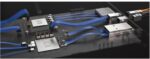
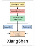
At the summit, S2C showcased its FPGA prototyping solutions with live demos across multiple RISC-V applications – including the Xiangshan processor running a graphical Linux interface. S2C has collaborated with Beijing Open Source Chip Research Institute (BOSC) since the first-generation Xiangshan CPU. In the recent validation of its third-generation Kunminghu processor – a 16-core RISC-V design with NoC interconnect running on two S8-100Q Logic Systems (each with 4 VP1902 FPGAs) were deployed and achieved a static timing closure at 12MHz. BOSC recognized S2C as a “Strategic Contributor” for its critical role in accelerating Xiangshan’s development cycle.
Additionally, Xuantie R908—a high-efficiency processor designed for real-time performance—was demonstrated live running on S2C S7-19P Logic System. The demo effectively demonstrated its low-latency operation and field-ready reliability.
Equally notable was Andes Technology’s 64-bit RISC-V vector processor IP core, the AX45MPV – running Linux and large language models easily efficiently on S2C’s S8-100 Logic System through the Andes Custom Extension (ACE) framework.
Overcoming Simulation Bottlenecks with Transaction-Based Acceleration
The RISC-V Verification Interface (RVVI) provides a standardized framework to ensure ISA compliance and functional correctness. Yet, as RISC-V designs grow in complexity—especially with custom extensions—traditional simulation methods encounter challenges like slow execution speeds, limited debug visibility, and difficulties scaling to full system-level verification.
To address these challenges, the keynote by Yang Dehao focused on Transaction-Based Acceleration (TBA), a verification methodology that enhances RVVI by decomposing test scenarios into reusable transaction flows. TBA leverages co-simulation between virtual prototyping platforms and hardware emulators—using tools such as S2C’s Genesis Architect and OmniArk/OmniDrive—to significantly improve verification speed and observability at scale, while maintaining RVVI compliance.
This approach exemplifies how advanced verification methodologies, combined with powerful prototyping tools, can accelerate the path from RTL validation to full-chip system verification.
Building on this, VP of marketing Ying J Chen highlighted S2C’s continued commitment to ecosystem collaboration and innovation:
“It is exciting to see thousands of engineers at the summit, and the manifestation of our partners’ RISC-V cores drawing a large crowd to our booth,” stated Ying J Chen, VP of Marketing at S2C. “We don’t just see ourselves as tool providers—we’re also an advocate for innovation and customers’ success. We’re committed to deepening our effort in the RISC-V community and broaden the ecosystem.”
S2C Inc. is a global provider of FPGA prototyping solutions for SoC (System on Chip) and ASIC (Application-Specific Integrated Circuit) designs. They offer hardware, software, and system-level design verification tools to accelerate the development process. S2C’s solutions are used for design exploration, IP development, hardware verification, system validation, software development, and compatibility testing.
Also Read:
Double SoC prototyping performance with S2C’s VP1902-based S8-100
Cost-Effective and Scalable: A Smarter Choice for RISC-V Development


