webinar banner AI 2026 v2

Mentor’s Symphony in Tune with AMS Designer Needs

Mentor’s Symphony in Tune with AMS Designer Needs
by Tom Simon on 11-14-2018 at 12:00 pm

Mixed signal simulation is a very hot topic these days. In modern designs, it is harder to draw a line between the analog and digital and work with them independently. Analog blocks are showing up everywhere. Even in what would have qualified as a digital design a few years ago, now designers need to look at things like PLLs, IOs and SerDes from a detailed analog perspective in context to ensure proper design behavior and performance. The drive to reduce power, the addition of sensors, increased use of ADCs, oscillators and other analog blocks in SOCs have all exacerbated the need for faster, easier and more accurate mixed signal modeling. At the same time requirements imposed by automotive standards such as ISO 26262 are creating the need for more comprehensive verification of mixed signal chips.

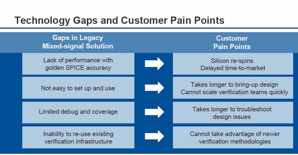
This last week Mentor has created quite a buzz with the introduction of their Symphony Mixed Signal Platform. Mentor has never been a slouch when it comes to analog and digital simulation. However, their AFS (Analog Fast SPICE) has been a game changer for the industry. What Symphony brings to the table is the ability to easily combine the leading analog simulator with Mentor’s, or other, digital simulators. At the same time Symphony overcomes many of the limitations that engineers faced while trying to verify mixed signal designs.

Typically, transistor level analog simulation was too slow to incorporate with digital simulations. As a result, people turned to behavioral models to speed up the analog side of the simulation. However, creating these models requires specializes skills and extra development time. And, of course any design revision required rework. Symphony lets design teams avoid the need for behavioral modeling to achieve faster run times. AFS provides nanometer SPICE accuracy and a capacity of 20M SPICE elements.

One of the key concepts of Mentor’s Symphony is their use of Boundary Elements (BE) that support all signal types and multiple power domains, including dynamic supplies. Their approach significantly improves debug, where now detailed information about signals at the interfaces can easily be examined in detail. Their approach is flexible enough that mixed digital and analog hierarchies are easily supported, with multiple levels and no restrictions on mixing A or D at each level. One important feature that Mentor is highlighting is their Hi-Z checking capability, which lets designers detect when a mixed signal net goes into a ‘Z’ state.

According to Mentor they have 30 customers who have been using Symphony prior to its release and their announcement contains many customer quotes reporting dramatic improvements in runtime and overall results.

Stepping back, this new product from Mentor is starting to paint a picture of what the Siemens acquisition means for Mentor. Going from a public company to a privately held company can mean big changes. I know that many people in the industry were wondering if Mentor would become the private EDA group for Siemens or if they would be able to continue robust product development. Much of Mentor’s more recent reputation and success has come from the Calibre line. Of course, Mentor has very competitive offerings across their product line. However, Symphony looks like a major long-term investment that aims to upset the analog mixed signal flow status quo. There is more information about Symphony on the mentor website.


Synopsys DDR5 LPDDR5 Memory Interface IP Targets AI, Automotive, and Mobile SoCs

Synopsys DDR5 LPDDR5 Memory Interface IP Targets AI, Automotive, and Mobile SoCs
by Camille Kokozaki on 11-14-2018 at 7:00 am

Synopsys announced on October 24 new DesignWare[SUP]®[/SUP] Memory Interface IP solutions supporting the next-generation DDR5 and LPDDR5 SDRAMs. The DDR5 and LPDDR5 IP significantly increase memory interface bandwidth compared to DDR4 and LPDDR4/4X SDRAM interfaces, while reducing area and improving power efficiency. The DesignWare DDR5 IP, operating at up to 4800 Mbps data rates, can interface with multiple DIMMs per channel up to 80 bits wide, delivering the fastest DDR memory interface solution for artificial intelligence (AI) and data center system-on-chips (SoCs).

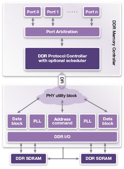
The industry’s first LPDDR5 IP, running at up to 6400 Mbps, provides significant area and power savings for mobile and automotive SoCs with its dual-channel memory interface option that shares common circuitry between independent channels. For additional power savings, the DesignWare Memory Interface IP solutions provide several low-power states with short exit latencies and offer multiple pre-trained states for dynamic frequency change capability. The DDR5 and LPDDR5 controller and PHY seamlessly interoperate via the latest DFI 5.0 interface, providing a complete memory interface IP solution for high-bandwidth, low-power SoC designs.

DesignWare DDR IP Solutions

[table] border=”1″ cellspacing=”0″ cellpadding=”0″ style=”width: 100%”
|-
| style=”width: 15.32%” | DesignWare DDR PHY(New)
(full list here)
| style=”width: 33.92%” | SDRAMs Supported /
Maximum Data Rate

| style=”width: 15.9%” | Interface to Memory
Controller

| style=”width: 34.86%” | Typical Application
|-
| style=”width: 15.32%” | LPDDR5/4/4X
| style=”width: 33.92%” | LPDDR5 / 6400 Mbps
LPDDR4 / 4267 Mbps
LPDDR4X/ 4267 Mbps
| style=”width: 15.9%” | DFI 5.0
| style=”width: 34.86%” | Design in 16-nm and below that requires high-performance mobile SDRAM support up to 6400 Mbps
|-
| style=”width: 15.32%” | DDR5/4
| style=”width: 33.92%” | DDR5 / 4800 Mbps
DDR4 / 3200 Mbps
| style=”width: 15.9%” | DFI 5.0
| style=”width: 34.86%” | Design in 16-nm and below that requires high-performance DDR5/4 support up to 4800 Mbps
|-

Some highlights:

  • The industry’s first LPDDR5 controller, PHY, verification, and IP solution support data rates up to 6400 Mbps with up to 40% less area than previous generations
  • The complete DDR5 IP solution supports up to 4800 Mbps with single, dual channels for discrete devices and DIMMs
  • Both solutions provide several low-power states with short exit latencies and offer multiple pre-trained states for dynamic frequency change capability

The DesignWare DDR5 and LPDDR5 IP solutions support all required features of the DDR and LPDDR specifications, enabling designers to incorporate the necessary functionality into their SoCs:

  • Firmware-based training via an embedded calibration processor in the PHY optimizes the boot-time memory training for highest data reliability and margin at the system level. It also allows fast updates to the training algorithms without requiring changes to the hardware
  • Decision feedback equalization (DFE) used in the input receivers reduces the impact of inter-symbol interference (ISI) to improve signal integrity
  • Reliability, availability, serviceability (RAS) features, including inline or sideband error correcting code (ECC), parity, and data cyclic redundancy checks (CRC), reduce system downtime
  • Synopsys PHY hardening and signal/power integrity expertise enable faster design completion time and a higher design confidence degree.
  • Synopsys VIP for DDR5 and LPDDR5 provides randomized configuration and runtime selection, as well as built-in comprehensive coverage, verification plan, and protocol checks for increased productivity.

ARM, Micron and SK Hynix provided testimonials in a Synopsys press release on October 24, 2018. In that press release John Koeter, vice president of Marketing for IP at Synopsys, emphasized that Emerging applications such as AI, automotive, and cloud are requiring significantly higher memory bandwidth to address the massive amount of data throughput. He added that Synopsys is offering designers the fastest DDR5 and LPDDR5 IP solutions on the most advanced FinFET processes to deliver innovative products that are differentiated in bandwidth, power, and area.

Availability

  • The DesignWare DDR5 PHY and LPDDR5 PHY are scheduled to be available in Q1 of 2019
  • The DesignWare DDR5 Controller and LPDDR5 Controller are scheduled to be available in Q2 of 2019
  • The VC Verification IP for DDR5 and LPDDR5 is available now.

Worth Noting

  • All the DFI-compatible DDR PHYs are supported by Synopsys’ unique DesignWare DDR PHY Compiler. In addition, Synopsys’ DesignWare DDR5/4 Controller, LPDDR5/4/4X Controller, and Enhanced Universal DDR Memory and Protocol Controller IP feature a DFI-compliant interface, low latency and low gate count while offering high bandwidth. Optional market-specific features like AMBA AXI/4 AXI Quality of Service (QoS) and Reliability, Availability, and Serviceability (RAS) features allow you to match the area and capabilities of the controllers to designer needs.
  • Synopsys also offers DesignWare HBM2 IP, which provides 12x the bandwidth of DDR4 IP and ten times better power efficiency for graphics, high-performance computing, and networking SoCs.

DesignWare[SUP]®[/SUP] Memory Interface IP solutions


Fusion Synthesis for Advanced Process Nodes

Fusion Synthesis for Advanced Process Nodes
by Alex Tan on 11-13-2018 at 12:00 pm

Synopsys recently unleashed Fusion Compiler™, a new RTL-to-GDSII product that enables a data-driven design implementation by revamping Design Compiler architecture and leveraging the successful Fusion Technology –seamlessly fusing the logical and physical realms to produce predictable QoR. It is a long-awaited move that provides a breakthrough solution as more designers are migrating into deep advanced nodes, 7nm and beyond.

Let’s glance through earlier synthesis key challenges that might act as precursors to subsequent developments leading towards this vital product announcement.

Traditional synthesis challenges
As part of the RTL-to-GDSII flow, synthesis tool such as Design Compiler transforms design RTL description into an optimized gate-level representation. This includes performing architectural, logic and gate level optimization steps. Synthesis utilizes standard cell library, pre-characterized for timing and power across various input slews, load conditions and process corners (or PVT –Process, Voltage, Temperature), to generate optimal design based on a given set of PPA (Performance, Power and Area) target. Over time, synthesis has been fitted with limited physical and placement awareness as inroad into routing.

As wire performance fails to keep pace with device performance in advanced process scaling, inadequate interconnect modeling or estimation has translated to a disparity between the synthesis QoR and those generated by downstream physical implementation tools. The once tolerable trade-off across PPA during micrometer process node era is no longer acceptable for sign-off in advanced nodes –as designs are increasingly being targeted for emerging applications that require power efficiency as well.

Interconnect shift impacts not only on delay related metric, but also on power due to the increased RC or degraded-slew induced power dissipation. Such gap has been exacerbated by device threshold lowering or near threshold condition that shifts the total power contribution from dynamic to the static term. This drives the need of having a solution that delivers optimal results for both performance and power.

Moreover, increased design density also has strained synthesis tool and has demanded scalability, runtime improvements and more physical awareness. For example, the tool needs not only a congestion awareness but also a capability for generating legalized placement –to ascertain an accurate resource utilization and minimal perturbation during route optimization.

Common Data Model and Fusion Technology
Key to this breakthrough is the adoption of a common data-centric architecture. The Fusion Compiler single data model contains both logical and physical information to enable sharing of library, data, constraints, and design intent throughout the implementation flow. It has scalability to support ultra-large designs with the smallest feasible memory footprint. The Fusion Data Model serves all design phases and provides faster tool-data model interaction, interactive what-if analysis, and native multi-everything (cores, corners, etc.) with near-linear scalability across multiple CPU cores. It also supports transparent, multi-level hierarchy and the efficiency to run compute-intensive algorithms, facilitating more optimizations for better QoR.

Another enabler is Synopsys Fusion Technology™ which was announced in March 2018. It provides new level of integration of Synopsys synthesis, place & route and signoff tools, by redefining conventional product boundaries with systematic sharing of algorithms, code and data representations across multiple tasks.

Fusion provides Design Fusion, ECO Fusion, Signoff Fusion, and Test Fusion technologies. Design Fusion enables synthesis technology inside place-and-route, and place-and-route technology inside synthesis. ECO Fusion drives faster signoff closure with the signoff analysis and ECO optimization enabled directly from within implementation. Signoff Fusion eliminates design margin and over-design, using PrimeTime and StarRC for both optimization and signoff. Test Fusion is the combination of design-for-test (DFT), synthesis and automatic pattern generation (ATPG) technologies. Using physical design data, Test Fusion ensures optimal placement of test points while minimizing routing congestion and area impact.

Fusion Technology offers a bidirectional access between synthesis and the adjoining implementation tools, including sharing of optimization engines between the two domains. As Fusion Compiler integrates all synthesis, place-and-route and signoff engines on a single data model, it removes the necessity of having data conversion and transfer –hence, providing good QoR accuracy, best predictability and optimal throughput.

The Fusion Design Platform also AI-enhanced to enable additional QoR and TTR gains by speeding up computation-intensive analyses, predicting outcomes to improve decision-making, and leveraging past learning to drive better results.

Fusion Compiler QoR and Customer Feedback
The unified architecture of Fusion Compiler shares technologies across the RTL-to-GDSII flow delivering 20 percent better QoR and 2X faster time-to-results (TTR). It has been silicon-proven at several customers.

Fusion Compiler’s new solver-based global optimization engine enables path-based total negative slack (TNS) targets and analysis of critical path traces for effective design closures. Both pre- and post-route engines use the same costing and infrastructure for consistent correlation throughout the flow. Its underlying multi-corner multi-mode (MCMM) and multi-voltage (MV)-aware heuristic algorithms concurrently tackle all the design metrics for best QoR. Likewise, logic remapping, rewiring and legalization interleaved with placement minimizes congestion and speeds timing closure. The CTS engine follows a networking flow paradigm for optimal balancing of latency and skew.

“The power of this technology is essential for the design of tomorrow’s FinFET-based automotive applications. With Fusion Compiler, we achieved the target design goal and completed the tapeout. Compared to conventional technology, we confirmed a 33 percent reduction in timing violations, 10 percent area reduction, and 30 percent less leakage power, while cutting the design turnaround time in half. We have completed the integration of Fusion Compiler in Toshiba’s design environment and have begun to deploy it to upcoming SoC designs,” said Seiichi Mori, senior vice president, Toshiba Electronic Devices and Storage Corporation.

As shown in figure 2 and 3, Fusion Compiler runs produced more optimal PPA results from improved via-pillars handling and CCD (Concurrent Clock Data) optimizations –two snapshots of many underlying technological enhancements that promote the overall QoR gain.

“As design complexity increases across all our market segments, our key requirement is to achieve the best product performance coupled with the highest levels of predictability,” said Michael Goddard, senior vice president, Samsung SARC and ACL. “With Fusion Compiler, we are on track to achieve optimal PPA with up to 10 percent better timing, 10 percent lower leakage, two-to-five percent dynamic power savings, and typically two-to-three percent area reduction for our most challenging design blocks on our imminent tapeout. In addition, the predictable path from synthesis to signoff reduces design iterations, ensuring that we can meet our aggressive product schedules.”

“Strong semiconductor market drivers like autonomous driving and the adoption of AI continue to drive global demand for larger, faster, and more energy-efficient SoCs”, said Sassine Ghazi, co-general manager of Synopsys’ Design Group.

“Our early assessment of Fusion Compiler shows significantly better full-flow predictability, faster full-flow turnaround time, and better timing QoR compared to the previous approaches. We are collaborating with Synopsys to deploy this innovative RTL-to-GDSII solution, as it will streamline physical design of our mission-critical projects and allow us to bring new products to market much faster,” said Taichiro Sasabe, general manager, SoC Design Division at Socionext.

With this release of Fusion Compiler, Synopsys has raised the bar for a holistic synthesis solution –replacing the traditional RTL-to-GDSII design flow that is comprised of either disconnected or loosely-coupled tools for emerging applications and advanced process nodes.

For Fusion Compiler whitepaper please check HERE and datasheet HERE.


DAC 2019 to Host the Second System Design Contest!

DAC 2019 to Host the Second System Design Contest!
by Daniel Nenni on 11-13-2018 at 7:00 am

Interested in showing off your talent in developing deep learning algorithms on embedded hardware platforms for solving real-world problems? Join the second System Design Contest (SDC) at the 56[SUP]th[/SUP] Design Automation Conference in 2019!
Continue reading “DAC 2019 to Host the Second System Design Contest!”


IoT Security Process Variation to the Rescue

IoT Security Process Variation to the Rescue
by Tom Simon on 11-12-2018 at 12:00 pm

Unique device identities are at the core of all computer security systems. Just as important is that each unique identity cannot be copied, because once copied they can be used illegitimately. Unique device IDs are used to ensure that communications are directed to the correct device. And they also provide the ability to encrypt communication – an essential component for security of data in motion. Any device with a programmable ID can be cloned. The only way to limit this is to perform the programming as soon after fabrication as possible. However, programmable IDs still leave open a window of opportunity for misuse and add extra steps to the manufacturing process.


The number of IoT devices is expected to proliferate to nearly 50 billion by 2020. Each one needs security, most likely provided by an on-chip identifier. What if each device could contain a unique ID automatically, right at the point of manufacture, that could be used as the basis of a security system? This is the premise behind a Physical Unclonable Function (PUF).

As we know, there are minute variations in silicon chips due to manufacturing processes. Intrinsic ID, a software and hardware IP provider, has examined the wide range of techniques available to capture a repeatable yet unique ID from ICs. Eschewing methods that required analog circuity, the addition of special layers or the use of special processes, they settled on SRAM bit cell initialization states. Practically every IoT chip has SRAM and an embedded processor. Every SRAM bit cell will initialize to a 1 or a 0 depending on the precise threshold voltages of its transistors. It’s worth noting that some bit cells will fall within a range where the initialization state is not predictable, but there are methods to avoid or correct for these specific cells.

When the chip is powered off there is no trace of the unique ID left by a range of SRAM cells (volatile memory); as well, the unique ID is generated on demand and never stored. To date, analysis by security labs and customers have not been able to reveal any weaknesses in their system. Through a process called enrollment a PUF key is generated. This is used to create a public and private key for data exchange with external systems.

Small blocks of SRAM can be used to create 128-bit or 256-bit keys. Intrinsic ID has performed reliability testing over a wide range of conditions and also has done aging analysis to guarantee a lifespan of 25 years. Intrinsic ID’s PUF has been qualified for automotive, industrial and military uses through their work with customers and partners. Just as importantly, this IP’s unique operational invariance across technology nodes and fabs makes designer’s jobs easier.

The SRAM-based PUF from Intrinsic ID can be implemented with a small uninitialized SRAM block on chip and either an RTL IP block or embedded code that runs on chip; both approaches would need to have a proper security perimeter implemented. Intrinsic ID’s solution has gained excellent traction through a number of their customers and partners. Invensense created their TrustedSensor concept using this PUF. NXP offers SRAM PUF in its LPC and i.MX platforms for secure microcontrollers. Synopsys Designware uses SRAM PUF in their ARC EM Architecture for ultralow power embedded processors. Intel, Microchip, Renesas and Samsung also offer products that utilize SRAM PUF.

Intrinsic ID has written a white paper that is available on their website that goes into greater detail on the technology of their SRAM PUF. Unique unclonable keys are an absolute necessity for the profitable proliferation of the IoT. With this technology, devices used for personal or commercial applications are secure from hacking and data interception. It is easy to implement SRAM PUF without the need for special processes or dependence on analog IP. In closing I’ll say it’s nice to finally write an article about how process variation can serve a beneficial purpose.


Intel Diversity Semiconductors

Intel Diversity Semiconductors
by Daniel Nenni on 11-12-2018 at 7:00 am

Growing up in a military family, mostly in California, I would consider my cultural diversity life experience to be more than most. I remember in the 1960s some older folks were chattering about a colored family moving into our neighborhood and they had a son my age. Imagine my excitement as a child in having a multicolored friend! As it turns out he was only one color but we were fast friends anyway.

The other diversity experience I had growing up was with my mother. She wanted to be a mechanical engineer but that was a challenge for women in the 1950s and even more so after having children. She ended up being a draftsperson for a NASA contractor. I remember visiting her at work and getting some very cool Apollo NASA stickers and gifts. The other thing I remember is that all of the drafts people were women which seemed kind of odd to a young mind. Clearly I was never going to be a draftsperson because you had to be a woman so I decided to be an astronaut because those were all men.

My mother’s theme song was “Anything You Can Do I Can Do Better” from Annie Get Your Gun and that was the way she lived. She bowled in the PWBA when it first started and was a full on pool hustler. Her final job was at LAM Research, testing semiconductor equipment in Fremont. She really was a Rosie the Riveter of her era.

For my undergraduate degree I attended a University in Northern California that had nursing and teaching programs so the female to male ratio was higher than most but still the engineering classes were male dominant. There were some women in computer programming classes but hardware classes were again all men.

When I joined the semiconductor industry in the 1980s it was not diverse at all up until the fabless semiconductor transformation in the 1990s. Yet another thing we can thank Morris Chang and TSMC for. Today I would say the semiconductor industry is diverse (as compared to other technology based industries) and that diversity really is the core strength of the semiconductor ecosystem, absolutely.

The semiconductor diversity exception is a few old school IDMs lagging behind which brings us to Intel.

In 2015 Intel announced a Diversity in Technology initiative, committing $300M to accelerate diversity inside Intel. I guess I wasn’t shocked when I saw the diversity slides based on my personal experience with Intel but spending $300M for a quick fix to a years long problem seemed puzzling at the time. You can see the 2015 slides HERE. Intel released a diversity update claiming “full representation” in its workforce two years ahead of schedule. You can see the 2018 slides HERE:


And here is the updated Intel diversity blurb:

A diverse workforce and inclusive culture are key to Intel’s evolution and they are the driving forces of our growth. In addition to being the right things to do, they are also business imperatives. If we want to shape the future of technology, we must be representative of that future. In January 2015, Intel announced the Diversity in Technology initiative, setting a bold hiring and retention goal to achieve full representation of women and underrepresented minorities in Intel’s U.S. workforce by 2020. The company also committed $300 million to support this goal and accelerate diversity and inclusion – not just at Intel, but across the technology industry. The scope of Intel’s efforts span the value chain, from spending with diverse suppliers and diversifying its venture portfolio to better serving its markets and communities through innovative programs. Intel achieved its goal of full representation in its U.S. workforce in 2018, two years ahead of schedule. This achievement was the result of a comprehensive strategy that took into account hiring, retention and progression. However, Intel’s work does not stop here. We continue to foster an inclusive culture where employees can bring their full experiences and authentic selves to work.

So, let’s congratulate Intel on their diversity achievement. Hopefully now they can hire and retain the most qualified people without bias as to race or sex. Hey, wait, what about age diversity?


For Car Makers Google Scare Means It’s Time to Share

For Car Makers Google Scare Means It’s Time to Share
by Roger C. Lanctot on 11-11-2018 at 12:00 pm

Google says it wants to charge fees to handset makers in Europe for Android apps such as Googlemaps and Gmail, according to the New York Times. The move is clearly a reaction to the $5.1B fine imposed by the European Commission (and under appeal by Google) in reaction to Google’s perceived monopolist practices.

Is the scare of Google hegemony enough to convince auto makers they need to share data in the interest of preserving their independence?

A key motivation behind the $3.1B acquisition of map maker HERE from Nokia by Daimler, BMW and Audi was to ensure the independence of HERE and access to its maps for support of in-vehicle navigation systems, mobility services and autonomous driving development. In the ensuing three years, the venture has failed to attract any additional auto maker investors even as Audi, BMW and Daimler have proceeded to share vehicle sensor data and expand the HERE platform.

The abiding concern regarding Google, is the potential for the company to disrupt consumer relationships in the industry such that Google ultimately controls such key customer engagement points as service delivery, and content and application management and any related advertising or marketing opportunities. It all comes down to browsing and search which underpin Google’s $100B advertising portfolio.

The car is arguably the ultimate browser. Google wants to own that space.

Many auto makers have their own app platforms today, just as handset makers once did. In the handset space, most independent app stores were long ago eliminated by the dominant Google and Apple offerings. For auto makers the significance of the announcement is that it is a reminder of Google’s over-arching influence. It is enough to give pause to any auto maker considering the broader adoption of Google’s automotive services (i.e. Volvo, Renault) and to give impetus to those considering a tie-up with the HERE-Audi-BMW-Daimler venture.

The confrontation calls to mind the Microsoft Consent Decree arrived at in the U.S. nearly 20 years ago which forbid Microsoft from bundling its Internet Explorer browser with its operating system. By the time that agreement was reached the bundling of IE was a moot point and the importance of advertising was only just emerging.

Makers of Android-based smartphones had no initial comment for the New York Times to report, but the change will mean added cost for these devices that will have to either be absorbed or passed on to consumers.

Auto makers are watching developments closely, or should be, because the cost of implementing Android along with related Google provided services and applications is a key consideration behind adopting the operating system. And many auto makers are in the process of doing just that – sticking the Android operating system into their in-vehicle infotainment systems arriving in the market next year and beyond.

Implementing Android in cars is actually a relatively harmless process as no surrender of customer or vehicle data is necessary. Google has even intimated to auto makers that they will be able to add Google Voice to Android without surrendering customer control. But it may be time for auto makers to consider taking out some insurance in the form of a stake in the HERE joint venture. For its part, HERE will do well to give its best performance as a reliable alternative to Google.


Ford in DC Refining Autonomous

Ford in DC Refining Autonomous
by Roger C. Lanctot on 11-11-2018 at 7:00 am

When cities put on a press event to announce they are welcoming a company to town to test autonomous vehicles within the city limits the news is greeted with polite interest and some trepidation – as it was yesterday in Washington, D.C. There is an “oo-ah awesome” high-tech buzz immediately tempered by a “Why?” buzzkill.

In the case of Ford’s announcement in Washington, the spinmeisters got directly to the point. The introduction of autonomous Ford vehicles – 5-10 at first early next year in advance of a full on rideshare service fleet in 2021 – is intended to create jobs and re-training opportunities throughout the District’s eight Wards.

The press event included substantial representation and participation from the DC Infrastructure Academy which provides employment opportunities and job training for infrastructure-related jobs. DC Infrastructure Academy will help Ford’s effort by training vehicle operators and technicians. Additionally, Ford will open an autonomous vehicle terminal in Ward five and the company says it will work to train residents for auto technician careers that could involve self-driving vehicles in the future.

According to Ford, the training will be through courses developed by Excel Automotive in Ward 7 and Ford’s Automotive Career Exploration program with support from local dealers Chesapeake Ford Truck, DARCARS and Sheehy Ford of Marlow Heights. The involvement of dealers was an especially nice touch by Ford.

By emphasizing job creation, Ford and the DC leadership short-circuited the knee-jerk job-killing conversation associated with robo-cars. Better still for Ford, it diverted attention from the fact that the announcement will do nothing in the short-term to ease the traffic congestion in the city.

In essence, Ford is announcing that it is commencing its data gathering activities to prepare for autonomous operation in the city. The Ford vehicles will be nothing more than surveyors/mappers of the city – an operation already begun by Ford’s Argo team. It means that in the short-term Ford vehicles will be adding to the general glut of DC traffic.

Ford arrives in the wake of a report published by the National Capitol Region Transportation Planning Board – “Visualize 2045” – which anticipates a 46% increase in congestion in the Washington, DC area by 2045 and offers a $291B plan to mitigate the impact of that demand.

Quicker solutions are being sought by the DC Council, according to reporting by WAMU. The Council is considering:

  • Banning vehicle right turns on red at more than 100 intersections in the downtown business district and near school zones and cycle tracks within the next 18 months;
  • Eliminating areas where two lanes of traffic can turn left at the same time. The city has got rid of 15 of those intersections and plans four more by the end of 2018;
  • Doubling protected bike lanes from 10 to 20 miles and accelerating the construction of a dozen of those projects in the next three years;
  • Adding “hardened” medians to slow vehicles turning left, especially at intersections with a lage number of vehicles and pedestrians;
  • Expanding the District Department of Transportation’s pick-up and drop-off zones for ride-hailing vehicles and delivery to help reduce the amount of stopping in bike lanes and crosswalks. Five new zones will be added in places like the Wharf and 14th street.
  • Reducing speed limits in the city from 25 miles per hour to 20.

Robo cars from Ford (with safety drivers) on DC streets will join a panoply of transportation options which includes scooter and bike share operators (Bird, Lime, Skip, Jump, Spin and, the latest entrant, Lyft), along with car share companies: Maven, Car2Go, ReachNow and ZipCar. (Enterprise RideShare departed DC earlier this year.) DC can already boast several transportation-related firsts, not all good.

  • DC claims to be the first city to offer Starship delivery bots.
  • DC claims to have had the first shared scooter fatality in the U.S. – resulting from a crash with an SUV.
  • DC claims to be the first city to get Lyft’s shared scooter offering. (Lyft acquired Capitol BikeShare earlier this year.)

DC is the second city to get autonomous Fords, following Miami. Ford’s autonomous vehicles are also operating in Detroit and Pittsburgh.

Ford and DC are taking advantage of the lack of autonomous vehicle regulations in the District or the country. Washington, D.C, essentially stole a march on neighboring states Maryland and Virginia, both of which are angling for autonomous testers, but DC is first in the area to put such vehicles on public roads.

One would have thought the lack of autonomous vehicle regulations might have stimulated some safety advocate outrage at the open-air press conference held on the Wharf in Southwest DC. The Insurance Institute for Highway Safety is based just across the river in Arlington, Va., and the headquarters of the U.S. Department of Transportation along with the offices of a host of lobbyists were within walking distance of the event. Resistance to driverless cars was not represented. Perhaps resistance is futile when city representatives are seeking any and all solutions to a monumental traffic congestion problem increasingly framed by increasing fatalities.

DC traffic is unique thanks to the architect of its streetscape, Pierre Charles L’Enfant, who gave the city 22 traffic circles creating some unusual traffic management challenges. Of late, traffic fatalities involving pedestrians, bicyclists and buses, in particular, have been on the rise.

In sum, kudos to the Ford team for dodging the job-killer robocar angle and avoiding the dangerous driverless cars protesters. Treating the onset of robocars as a job creation and retraining opportunity is a novel and admirable approach – and one likely to be replicated elsewhere. Echoes of Uber’s fatal crash in Phoenix, earlier this year, were faint on the Wharf in Washington.


Webinar: NVIDIA Talks High Quality Metrics in Power Integrity Signoff

Webinar: NVIDIA Talks High Quality Metrics in Power Integrity Signoff
by Bernard Murphy on 11-09-2018 at 12:00 pm

There’s a familiar saying that you can’t improve what you can’t measure. Taking that one step further, the more improvement you want, the more accurately you have to measure. This become pretty important when you’re building huge designs in advanced technologies. Margins are a lot tighter all round and use-cases are massively more complex, potentially hiding all kind of dangerous corners. In such cases, you really need to do a very comprehensive analysis across multiple variables to find the right bounding conditions and to avoid massive overdesign by managing corrections as surgically as possible. Join this webinar to lean how NVIDIA does just that using ANSYS RedHawk-SC’s elastic compute scalability and big data analytics.

REGISTER HERE for this webinar on November 28[SUP]th[/SUP], 2018 at 9AM PST

Summary
The availability of ubiquitous data and compute power to solve seemingly unsolvable problems is driving the artificial intelligence (AI) revolution in high tech today. Semiconductor chips for next-generation automotive, mobile and high-performance computing applications — powered by AI and machine learning algorithms — require the use of advanced 16/7nm systems-on-chips (SoCs), which are bigger, faster and more complex. For these SoCs, the margins are smaller, schedules are tighter and costs are higher. Faster convergence with exhaustive coverage is therefore imperative for first-time silicon success. A big data-enabled simulation platform that offers elastic scalability is required for enabling rapid design iterations to create a robust power grid design. Multivariable analytics and machine learning technologies are key for gaining valuable insights from the vast amount of simulation data to accelerate design closure.

In this webinar, leading semiconductor company Nvidia will discuss the limitations of traditional voltage drop analysis methodologies and share how ANSYS RedHawk-SC’s elastic compute scalability and powerful data analytics can be leveraged to accelerate next-generation SoC power integrity and reliability signoff. A new workflow using multivariable analytics, which considers grid criticality, timing criticality and simultaneous switching noise, is used for predicting the worst, local dynamic voltage drop (DvD) hotspots without running any transient simulation. This enables early detection of hotspots and offers feedback to the physical design team, making it possible to address design issues without impacting the tapeout schedule. The issues identified by this new flow were found to correlate well with vector-based dynamic voltage drop analysis with much faster turnaround time.

Speakers:
Kritika Garg, Nvidia
Currently working on IR drop signoff flow/methodology at Nvidia Corporation in Santa Clara, Kritika is an alumna of the University of Southern California with an M.S. degree in electrical engineering focused on digital VLSI system design and CAD. She has five years in the semiconductor industry, and previously worked as a block implementation design engineer with RTL-GDSII responsibilities at NXP Semiconductors (formerly known as Freescale Semiconductors) in India, and was a former intern in CAD methodology with the Silicon Engineering Group at Apple in Cupertino, California.

Sooyong Kim, ANSYS
Sooyong is a senior area technical manager with responsibilities for the new big data platform ANSYS RedHawk-SC and worldwide customer engagement. After joining Ansys in 2008 as part of Apache Design, he has held various positions in field operations. Previously, he worked at Cadence Design Systems and received a B.S.E.E. and a M.S.E.E. from Rensselaer Polytechnic Institute, Troy, New York.

About ANSYS
If you’ve ever seen a rocket launch, flown on an airplane, driven a car, used a computer, touched a mobile device, crossed a bridge, or put on wearable technology, chances are you’ve used a product where ANSYS software played a critical role in its creation. ANSYS is the global leader in engineering simulation. We help the world’s most innovative companies deliver radically better products to their customers. By offering the best and broadest portfolio of engineering simulation software, we help them solve the most complex design challenges and engineer products limited only by imagination.