webinar banner AI 2026 v2

ARM Spins New IP for Client Applications

ARM Spins New IP for Client Applications
by Bernard Murphy on 06-20-2019 at 5:00 am

Arm is a machine. They crank out new products in a wide range of categories, Project Trillium for AI, Neoverse for infrastructure, their Automotive Enhanced line and the Pelion IoT platform. And in each they have a regular beat of new product introductions following roadmaps they have already laid out. Not that you’d expect any less from a company in their position. Nevertheless, that they continue to deliver and expand high volume innovation pretty much as they forecast underlines that this is not a company resting on its laurels.

Ian Smythe VP Marketing for the client LOB announced three new IPs last month, directed particularly at mobile devices and the opportunity 5G is creating in those devices. Ian made an interesting point about AI and mobile which I hadn’t realized. I’m generally pretty dismissive about CPU-hosted machine-learning (ML) as the bottom end of the ML hardware hierarchy, but he pointed out that 85% of ~4 billion smart phones are running ML workloads without any dedicated ML hardware assist, using in many cases just CPUs or CPUs plus GPUs. Makes sense – ML hardware on phones is still a pretty new concept and an added cost, so continuing to push CPU-based and GPU-based support for mobile is still very worthwhile.

The first of the IP introduced was the Cortex-A77, building on the A76 architecture but offering a 20%+ advance in instructions-per-cycle performance, still very much targeting smartphone power envelopes and area. Arm sees these devices being particularly helpful in supporting emerging use-cases such as VR/AR/MR (collectively xR) and more advanced ML applications. Ian pointed out an interesting trend in performance for the A-class devices. Arm spent about 4 years, up through around 2016, doubling performance over the A15 but they doubled performance again in the following 2-3 years up to the A77. So they’re accelerating performance improvements while still keeping to mobile client efficiency (power, area) targets.

The next IP up was the Mali-G77. This is also based on an architecture change over the G76, delivering 40% higher performance over that earlier system. This new platform also manages to provide 30% better energy efficiency and 30% better performance density (more performance in a smaller area which is important given the generally large footprint of GPUs in mobile SoCs), along with an improvement in ML performance of 60%. So lower power, smaller area and faster object recognition.

Finally Ian introed the Mali-D77, a second-generation display technology based on their Komeda architecture and targeted particularly to untethered head-mounted displays. This is one of those many domains, almost everywhere, where a general-purpose solution (in this case a GP-GPU) could do the job, but intelligent offloading can do that job so much better. A smaller more dedicated device can do the job of managing display at lower power than the GPU and it can do it faster. The latter is rather important in HMDs because delays between body movement and perceived movement in the display are known to cause motion sickness. So less feeling groggy in your headset and smaller, lighter headsets makes for bad news for your pharmacist and chiropractor but good news for general health.

Ian said that these IPs are available for licensing, early access customers are already designing them into products, and he expects the first of these products to appear in 2020. Good advances, should be a real plus for a fuller mobile 5G experience: gaming, HD video, better voice control and generally more intelligent interfaces on-the-go.


SiP is the new SoC @ 56thDAC

SiP is the new SoC @ 56thDAC
by Tom Dillinger on 06-19-2019 at 6:48 pm

The emergence of 3D packaging technology has been accompanied by the term “more than Moore”, to reflect the increase in areal circuit density at a rate that exceeds the traditional IC scaling pace associated with Moore’s Law.  At the recent Design Automation Conference in Las Vegas, numerous exhibits on the vendor floor presented unique packaging options.  Yet, advanced packaging technology also requires corresponding methodology flows, spanning all facets of design, implementation and (electrical plus thermal) analysis.  I had an opportunity to catch up with John Park, Product Management Director for IC Packaging and Cross-Platform Solutions at Cadence, to talk about the flow requirements for these packaging solutions.

Taxonomy – SoC’s, SiP’s, and Chiplets

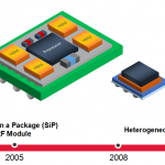
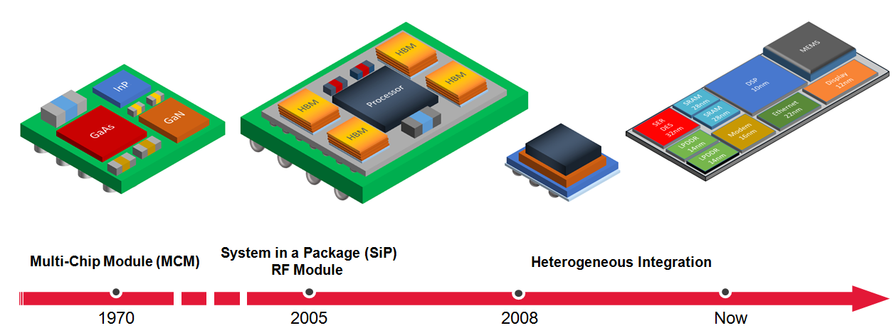
To start, I asked John for his insights on how to best understand the different terminology used to describe these package offerings.  He began using the image below:

John said, “Multi-chip module (MCM) technology has been around for decades, applied to very specific high-performance computing, communications, and aerospace applications.  The engineering resources to develop the physical implementations were considerable, as was the investment in chip-package-system electrical analysis.”

John continued, “This was followed by two trends.  The ongoing silicon technology scaling of Moore’s Law led to the introduction of system-on-chip (SoC) architectures, integrating IP from multiple sources.  Correspondingly, the signal and power I/O count of these die increased, as well.  The introduction of 2.5D packaging technology, with aggressive interconnect line/space pitch on an interposer (or substrate) enabled these high pin count die to be integrated on a complete system-in-package (SiP).  SiP opportunities have continued to expand.  The introduction of 3D packaging with vertically-stacked die using through-silicon vias (TSV’s) is a recent offering – this technology presents unique constraints to EDA flows, from (limited) pin access for test to different thermal modeling requirements.” 

“I’ve heard a lot recently about chiplets.”, I said.   “What’s a chiplet?”

John replied, “The next trend in SiP design is the integration of heterogeneous chiplets.  It is likely the case that not all functionality in the system needs the PPA characteristics of the same process node.  There may be cost and schedule advantages to the integration of (hard) IP functionality from different sources and technologies – these silicon IP’s are chiplets.  The chiplet I/O’s are simply microbuffers, with an appropriate test wrapper definition.  Chiplets represent a foundry and process node independent disaggregation of the IP in an SoC.  In short, the SiP is the new SoC”.

I asked, “Today, there are some (de facto) architectural definitions for interfacing the IP integrated in an SoC.  How will this extend to a chiplet-based SiP?”

John indicated, “There is a great deal of activity to establish a comparable architectural definition for chiplet based designs – perhaps the best known is the “Advanced Interface Bus” (AIB) specification that Intel has recently provided (license royalty-free).” 

AIB is a parallel bus, clock-forwarded definition for the physical layer interconnect between chiplets, similar to the parallel interface of a DDR DRAM memory module (with single data rate for control signals, double rate for data transfers).  The parallel interface suggests that the connections on the SiP will be “electrically short” and that the available chiplet bumps will be sufficient for parallel bus communications – the additional complexity of SerDes design and the related signal integrity analysis is not required.  Here is a site with more information about AIB, including a download of the specifications (link – registration required for download).

Note that there is also a DARPA program focused on defining a similar IP-chiplet design and reuse platform – “Common Heterogeneous Integration and Intellectual Property Reuse Strategies”, or CHIPS (link).

John added, “There will also be a significant focus on the verification IP (e.g., the verification compliance testbench) for chiplets on an SiP.”

I thanked John for the very lucid description of the nascent chiplet-based design strategy (and for the title of this article).  We shifted gears to discussing how these SiP technologies have impacted EDA tool and flow development.

SiP Reference Flow

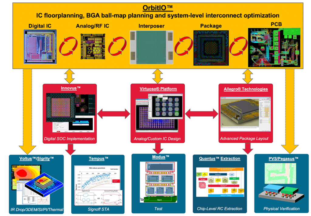
The release of a new silicon process design kit (PDK) by a foundry commonly also includes a description of the EDA platform tools that have been qualified for the process node – i.e., the “EDA reference flows”.  John indicated that advanced SiP design kits are also being accompanied by corresponding reference flows.  He described a recent collaboration with TSMC, to provide a comprehensive design and electrical analysis tool suite for TSMC’s advanced (2.5D and 3D) package offerings – e.g., CoWoS, InFO, WoW, and SoIC.  Here  is a list of some of the reference flow tools described in that collaborative announcement, with a few words on their interoperability for SiP designs (link):

Specifically, John focused on the recent enhancements to the OrbitIO interconnect designer.  “The diverse nature of the SiP silicon and package technologies necessitates using different tool platforms.”, John said.  “The methodologies that have been used to manage the overall SiP design tend to be rather ad hoc – for example, spreadsheets exchanged between engineering teams to represent the connectivity between silicon die microbumps, interposer routes/vias, through-silicon vias, and package bumps.  A single, consistent interconnect manager is needed to represent and maintain this model – that is the role of OrbitIO.”

John continued, “OrbitIO provides the SiP model across the platforms used for implementation and analysis of digital die, AMS die, and the package/PCB.  Note that the data representation between OrbitIO and each platform is bidirectional – there is direct integration with the platform to exchange the planning and implementation data.  As additional detail  and/or revisions are made in the specific platform, the updates are reflected in OrbitIO.”

“Are there model connectivity checks available in OrbitIO?”, I asked.  “Sourceless and sinkless pin checks, for example.”

“Yes.”, John replied.  “Further, there are extensions available for customers to develop their own rules and checks.”

There is definitely growing momentum for SiP designs, leveraging advanced 2.5D and 3D packaging technologies.  A significant percentage of those designs will integrate chiplet-level IP – look for standards to emerge for the interconnect fabric (and test methods) between chiplets.  To leverage the packaging technology, a comprehensive EDA strategy is required, to enable planning, implementation, and analysis across different engineering domains as well as to provide a complete, consistent SiP model across tool platforms.  For more information on how Cadence has approached the support for complex SiP’s, please follow this link.

-chipguy


#56DAC – Functional Safety Panel hosted by Mentor

#56DAC – Functional Safety Panel hosted by Mentor
by Daniel Payne on 06-19-2019 at 5:28 pm

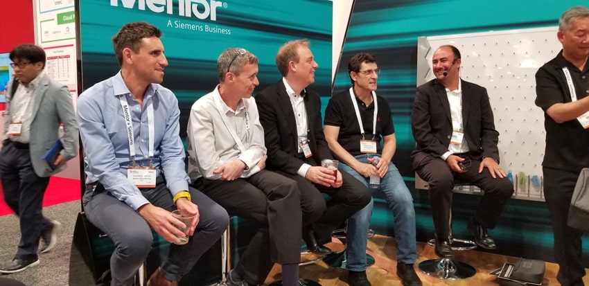
Four experts in the discipline of functional safety were gathered together at #56DAC in Vegas earlier in June, hosted at the Mentor booth, so I rested my legs and typed notes as fast as I could. The product areas that I first think about when functional safety (FuSa) comes up are automotive, medical and aerospace, because keeping human life protected in these areas is paramount. Our moderator was Bryan Ramirez from Mentor, and the panelists included:

The big picture is that automotive safety has gone far beyond just braking and ECUs, think ADAS and Autonomous Vehicles. There are now many new entrants in the automotive electronics space, and they certainly need to quickly learn about about safety practices.

Q: What is the state of the industry for tools to help FuSa requirements?

Ghani – we must meet safety requirements, but how do we achieve that at the system level? With autonomous driving how do we know that with the ML algorithms that it will detect obstacles properly? We need to collaborate in the industry in order to make autos safer. Tools are not complete yet, so there’s progress yes, but problems are growing so fast with AV.

Yves- we need to get suppliers all involved, working together on all ICs, sharing information, sharing IP information while keeping secrets. On the digital side we have good tools for safety, however on the AMS side we need better analysis and tools.

Nir – yes, analog is very complicated. FUSa today is like verification 20 years ago, and the tools are lagging. I really don’t want to wait 20 years to get FuSa tools.

Matt – we now have requirements management, system analysis and verification. Aerospace has many years experience for FuSa, so automotive is still catching up to that level. The tooling not mature yet for functional safety EDA tools and methodology.

Q: What about collaboration aspects?

Matt- to reach autonomous vehicles, safe systems requires collaboration across IP, automotive and systems companies in order to meet ISO 26262 requirements. How will we use these methods and apply new tooling?

Nir – We really need government input in order to meet our safety requirements.

Yves – with new process nodes the safety requirements change, so we need to collaborate with the foundries.

Ghani – within EDA we could use IEEE standards and communications to become safer. We already have Design For Man, DFT and now we need Design For Safety.

Q: How can I know when I’ve tested enough to be safe?

Ghani – well, following ISO 26262 for chip or IP is a minimum starting point, but there is no simple recipe on how to ensure safety in a product. There’s no such thing as complete validation. With safety when human life is in the balance the methodology is to do more verification than before, so it’s going to be company specific.

Yves- that’s a very important question, so the answer is to simulate, verify, then stop, but where is your plan? The plan is the starting point. Did I verify my requirements well? Fault injection simulations are required. Engineering judgement on top of simulation and verification is need, yet we need to go even further.

Nir – I agree, we need to first define our safety goals, then cross checking that we met each safety goal, just like when doing verification.

Matt – when do I know that I’ve verified enough? Has all of my IP been verified up to SoC and system level? Proving that the entire system has been validated is our real goal.

Q: Has my OEM supplier adhered to safety standards?

Matt – integrating each IP needs to fulfill all safety concepts. As each level in the design is completed, validation needs to happen.

Nir – I don’t know that users of our chips can validate what we’ve done internally to meet safety standards.

Ghani – design bugs can be either digital or analog, so how do I know that my verification has covered all of the bugs? At ARM with have used Bus Functional Models along with sensor models to mimic actual behaviors, and it must be highly accurate. Most OEMS just run software on a system, so they only need a high level model of our designs.

Q: How well does requirements get fed through the design chain?

Ghani – we don’t know all of the customer use cases, so we have to make assumptions. If tier 1 and OEMs can share more of what they need, then we could make safer IP blocks.

Yves – requirements need to reach the suppliers very early in the process. It’s not easy to define the requirements for safety. If we don’t get requirements soon enough, then our IP cannot meet expectations.

Matt – exchanging requirements between two different levels is a challenge, although there are multiple formats being used IPDF, Excel, etc., so there’s not a consistent method from top to bottom levels.

Yves – with the ISO 26262 standard we now have the same language to talk with all of our vendors.

My Take

They say that it takes a village to raise a child, and so it is with functional safety, because it will take close collaboration between the systems companies creating each new generation of cars and planes along with all of their suppliers: Foundries, EDA vendors, IP providers. At an annual event like DAC we do get to see all of these companies gathered together at one point in time, and having this kind of a panel discussion is one way to build awareness for our functional safety challenges and approaches.

Related Blogs


Meet the Experts @ ES Design West!

Meet the Experts @ ES Design West!
by Daniel Nenni on 06-18-2019 at 10:00 am

SEMICON West and ES Design West are right around the corner here in San Francisco and I wanted to point out the Meet the Experts segment in the appropriately named Meet the Experts Theater. Great idea really and a super great line-up. The best part of course is actually meeting the experts. Over my 35 year semiconductor career I have traveled more than a million miles and met thousands of the most intelligent people in the world. Never am I the smartest person in the room, not even close, which has made me an excellent listener, absolutely. Even my beautiful wife will tell you that I am a good listener, maybe.

Two more things, my favorite blues musician Aart de Geus has a keynote in the AI Design Forum that you are not going to want to miss and of course the Beyond Hot Party on Tuesday night at Johns Colins Lounge. My wife and I hope to see you there!

Meet the Experts
Tuesday — 10:30am-12:30pm
MORE THAN MOORE: As we reach the limits of scaling geometries, this
session will explore new ways to continue to increase system
functionality while reducing cost and size.
https://bit.ly/2WFsMal

Meet the Experts
Tuesday — 1:30pm-4:30pm
DESIGNING FOR LOW ENERGY: As Smart devices become more ubiquitous,
many have very stringent energy requirements, whether it be very long
battery life or harvesting energy from the environment. This session
will explore how designing for low energy is continuing to evolve with
new design techniques, IP and software solutions.
https://bit.ly/2IgHZL4

Meet the Experts
Wednesday — 10:30am-12:30pm
SILICON DESIGN IN THE CLOUD: As costs both for owning the tools and
the networking infrastructure used for designing (including
verification and modeling) of silicon dramatically increase, companies
are increasingly looking for cloud-based solutions on which to do
their silicon design. This session will chart the current and future
of such cloud-based design from the perspective of silicon design tool
users, developers of such tools, and cloud solution providers.
https://bit.ly/2WBNoQU

Meet the Experts
Wednesday — 1:30pm-4:30pm
MACHINE LEARNING, AI, AND EDA: From EDA tools to voice and image
recognition, machine learning and AI are increasingly important for
both the design and the design process. This session will explore the
impact on applications and tools.
https://bit.ly/2Iygrje

Meet the Experts
Thursday — 10:30am-12:30pm
SECURITY: With SoCs increasingly used in critical applications, and
more of the system software being integrated onto those chips,
hardware and software security becomes increasingly critical for
designers. Speakers will discuss security concerns and risks in
today’s designs.
https://bit.ly/2MH4VY7

Meet the Experts
Thursday — 1:30pm-4:30pm
ADVANCED APPLICATIONS: From DSP and media processing through changing interface standards, SoCs continue to increase in complexity. This
session will explore tools and methodologies to develop these complex
chips, along with advanced verification methodologies to assure
correctness.
https://bit.ly/31s0R1o


Synopsys Low Power Workshop Offers Breadth and Depth

Synopsys Low Power Workshop Offers Breadth and Depth
by Bernard Murphy on 06-18-2019 at 5:00 am

Synopsys seems to particularly excel at these events, whether in half-day tutorials at conferences or, as in this case, in a full-day on-site workshop. You might think there’s not much that can be added in this domain, other than to bring low-power newbies up to speed, but you’d be wrong. This event set the stage with surveys on needs in power management and verification (maybe this was for the newbies but good to recap), a detailed look at implementation aspects, the emerging importance of pre-RTL UPF checks, a very enlightening discussion on the scalability of UPF for large designs (hint – this is a problem) and a discussion on on-going work to attack that problem.

Power verification, optimization

There were also a couple of customer presentations, one from Intel and HYGON. In deference to the wishes of both companies I won’t discuss their presentations. I also won’t cover every Synopsys presentation to keep this blog to a manageable size.

Low Power Trends

Sridhar Seshadri (VP and Chief Architect at Synopsys) opened with an overview. Their customer verification surveys show low-power verification neck-and-neck with debug as the top verification concerns in 2018. Initiatives they have to manage the need include software-driven power analysis and signoff power closure. Mostly well-known flows here: ZeBu and Virtualizer for early analysis, ZeBu and PrimePower for peak and average analysis on RTL, and PrimePower and RedHawk for power and IR-drop signoff.

Mary Ann White (Dir Marketing in Synopsys DG, also an ISO 26262 functional safety practitioner) presented results from their customer survey, showing for example that while timing closure, timing and area goals and on-schedule tapeout lead all other concerns by a 2X+ margin, power concerns follow right behind. One very interesting insight was a side-by-side comparison of mobile and automotive expectations. In order of mobile and automotive:

    • process – 28nm to 7nm versus 180nm to 7nm
    • design size (instances) – 100M+ in both cases
    • frequencies – up to 4.2GHz versus up to 77GHz
    • voltages – 0.5 to 1.8V versus 1 to 60V
    • temperature – 0 to 40 degrees versus -40 to 150 degrees
    • expected lifetime – up to 3 years versus up to 15 years
    • target field failure rate – <10% versus zero

Automotive has caught up on process and size, is ahead on frequency, a wider span on voltage, and unsurprisingly more demanding on temperature, lifetime and failure rates.

Progress in Implementation

Mary Ann mentioned a number of power saving techniques available in the Synopsys implementation flow, including concurrent clock and data optimization, intelligently relocation ICG gates closer to the driver, more multi-bit banking and de-banking support, low power restructuring in DC NXT and in fusion between ICC II and synthesis, optimization in PT and ICC II for ultra-low voltage operation and optimizations in power recovery at signoff by downsizing or swapping cells on Vth. Each of these is delivering meaningful improvements in dynamic and/or leakage power savings.

Viswanath Ramanathan introed support for multiple power domains in a single voltage area with a couple of examples. I’m not going to butcher his technical explanation here – contact Synopsys for more detail.

UPF Scalability for SoC

Harsh Chilwal (PE at Synopsys) gave a fascinating and somewhat concerning presentation on the scalability of UPF. We all know that designs are getting bigger and so of course UPFs are getting bigger. What may be less apparent is how quickly at the SoC level UPFs are getting bigger and more costly to compile, at seemingly a super-linear rate even on a log-scale of UPF complexity. Harsh told us that this is the nature of the beast, mapping essentially flat Tcl (the foundation under UPF and most things EDA) onto structural RTL. This can only happen effectively after the design is resolved and can amount to 4X+ of total elaboration time for a VCS simulation.

Flexible though UPF is, that flexibility often fights efficiency. Loading UPF files (sometimes many nested files) for every relevant instance creates zillions of UPF objects, chewing up compile time and memory. Transitive find commands, beloved by many users for their adaptability, create huge strings which can easily overflow in a good-sized SoC and are correspondingly expensive in time and memory (blame Tcl, not UPF for that). Path-tracing, needed again for adaptability, can equally be hugely expensive in an SoC if not carefully bounded. These and other factors highlight the challenging tradeoffs between ease of use and practical bounded use in UPF-based applications.

Harsh suggested a number of methodology best practices to avoid or at least mitigate some of these problems, for example using wildcards rather than find_objects and using soft or hard macro attributes to identify IPs and thereby bound path-tracing. He also suggested using power models to make the UPF modular rather than flat and bind those models to the RTL, avoiding a lot of redundancy. He also talked about some forward-looking work they are doing on hierarchical compile as a way to break free of the flat UPF paradigm.

Kaushik De (Scientist at Synopsys) followed with an abstraction approach, a likely unavoidable tradeoff as designs and UPFs continue to grow. For this purpose, they define a signoff abstract model (SAM) which he positions as similar to a flat model, minus the things you don’t need to know (the devil is no doubt in those details); they have mechanisms to create, write and read SAM models. Kaushik also showed customer stats with significant run-time and memory improvements exploiting SAM-based flows.

The trick with hierarchical analysis is to ensure you can trust that nothing falls through the hierarchical cracks. He showed a couple of approaches they use to build confidence in the validity of the SAM-based analyses. Each compares abstracted analyses with full-flat analyses to ensure no violations are lost. Any disconnects are used to refine the SAM models I presume. I understand that customers using these flows today do the both analyses and comparison on an initial run, then use hierarchical analysis for subsequent runs, perhaps adding a full-flat run at the end for security.

Machine Learning in Low Power

It’s happening everywhere else; no surprise ML should appear here also. Mary Ann first talked about ML optimization for PrimeTime power recovery, achieving run-time speedups of between 4X and 10X. This is a supervised learning approach I was told. You, the customer, first train the system then can use that training on subsequent designs.

Kaushik talked about accelerating debug using machine learning. This I thought was a very cool application since it builds on unsupervised learning to identify clusters of related problems, unlike many ML applications which rely on supervised learning to identify specific object matches. This is particularly useful in static UPF analysis which can generate hundreds of thousands of errors. But there aren’t really anywhere near that many root-cause bugs; instead each real bug spawns many symptoms. Using unsupervised learning (with no doubt a good deal of secret sauce) can massively reduce the debug effort. Kaushik showed one example, resulting from a level-shifter error, where a huge number of reported errors and warnings could be traced back to just two problems. Way easier than the traditional approach.

You can learn more about what Synopsys is doing in low-power HERE.


An Update from Joe Sawicki @ Mentor, a Siemens Business 56thDAC

An Update from Joe Sawicki @ Mentor, a Siemens Business 56thDAC
by Tom Dillinger on 06-17-2019 at 10:22 pm

Executives from the major EDA companies attend the Design Automation Conference to introduce new product features, describe new initiatives and collaborations, meet with customers, and participate in lively conference panel discussions.  Daniel Nenni and I were fortunate to be able to meet with Joe Sawicki, Executive Vice President of the IC EDA segment at Mentor, a Siemens business, for a brief update.  Here are some of the highlights of our discussion.

Machine Learning in EDA

There were numerous technical sessions and EDA vendor floor exhibits relating to opportunities to incorporate machine learning algorithms into design automation flows.  Joe shared some examples where ML is being integrated into Mentor products:

  • Calibre Litho Friendly Design (LFD)

Lithographic process checking involves evaluating a layout database for potential “hotspots” that may detract from manufacturing yield.  Although conventional design rule checking will identify layout “errors”, there remains a small, but finite, probability that a physical design may contain yield-sensitive topologies at the edges of the litho process window.  Traditionally, lithographic process checking utilized a detailed litho simulation algorithm applied to the layout database – a “model-based” approach.

However, that method has become computationally intractable at current process nodes.  Instead, a “fuzzy” pattern matching technique was pursued, using a set of “hotspot-sensitive” layout patterns provided in the foundry PDK.  A set of “rule-based” checks were applied using these patterns.  More recently, a mix of model-based and rule-based techniques are used, where a subset of patterns find layout structures to direct to the litho simulation tool.  Yet, pattern identification is difficult.  It relies upon the (growing) database of hotspot identification, and a judicious selection of the pattern radius – too large a pattern will result in fewer matches and poor coverage, too small a pattern will identify many unnecessary hotspots for simulation.

Joe indicated, “Machine learning technology has been integrated into the Calibre LFD tool, to better distinguish which pattern structures are potential litho risks using training set learning.” 

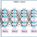
The figure below depicts a deep neural network applied to the binary classification of design patterns to direct to litho simulation (from the Mentor whitepaper:  Elmanhawy and Kwan, “Improve Lithographic Hotspot Detection with Machine Learning”).

Pattern matching and litho simulation rely upon an existing database of known hotspots.  Using a deep neural network, using hotspot and non-hotspot training data, the ML-based approach in Calibre LFD predicts additional yield detractors in new layout, beyond the pattern set in the PDK.  Very cool.

  • Calibre mlOPC

Joe continued, “We are also incorporating ML technology into the Calibre products used directly by the fabs.  There is a wealth of metrology data taken during fabrication.  We are applying pattern decomposition and classification on this data to provide feedback to the process engineering team, for process line tuning/centering and for optical mask correction algorithms.”

  • Tessent Diagnosis

Lastly, Joe described how ML methods are being applied in the area of fault diagnosis.  He indicated, “Mentor has led in the introduction of cell-aware test, where additional circuit node and parametric fault candidates within cells are presented to the test pattern generation and fault simulation tools.  We have incorporated ML inference techniques within Tessent Diagnosis to correlate test fail data, and provide improved cell-internal diagnostics to the physical failure analysis (PFA) engineering team.” 

There’s no doubt that ML technology will offer EDA developers new techniques for inference classification in analysis flows (and potentially, new approaches to non-linear optimization algorithms in design implementation flows).


Automotive System Verification and Digital Twin Modeling

There continues to be synergistic product developments within Siemens, leveraging the IC design and verification technology from Mentor.  (I presume any questions about the motivation behind the Mentor acquisition by Siemens have long since been answered.)

Joe described a recent Siemens announcement – the “PAVE 360” initiative – which provides a comprehensive (pre-silicon) verification platform for simulation of an automotive environment.

Joe said, “With the Veloce Strato emulation system, we have the capability and capacity to provide a digital twin of the automotive silicon design, the embedded software, the sensor/actuator systems, and the surrounding traffic environment into which the ADAS or autonomous vehicle is placed.  This includes both the deterministic and predictive (ML-based) decision support within the model.”

Joe also reminded us, “A digital twin environment is used not only for pre-silicon verification – it is also the debug platform to analyze field data.  Testing of autonomous driving solutions will uncover issues, providing engineers with an accident database.”

The ISO26262 standard for autonomous vehicles mandates a closed-loop tracking system that demonstrates how these issues have been addressed and subsequent verified.  The PAVE 360 digital twin platform is the means to provide that qualification.

The overall goal of the Siemens PAVE 360 platform is to provide a verification reference solution across the breadth of automotive sub-system suppliers.  A number of demonstration labs have been established worldwide, providing suppliers with access to the platform – see below.

More info on the PAVE 360 initiative is available here.

Photonics

In our remaining minutes, Joe highlighted another recent Mentor announcement, focused on accelerating the design and verification of silicon photonics layouts.  Conventionally, layout design consisted of placement of cells from a photonics library, followed by manual custom layout generation of the “waveguides” between the cells (and the related electrical signals that modulate the waveguides).  There are strict constraints on the length and curvature of the guides to minimize dispersion – photonic layout design has required specialized layout expertise.

Joe described the new LightSuite Photonic Compiler platform, developed with collaborative support from Hewlett-Packard Enterprise.  The compiler provides automated generation of the waveguide layouts and connections, as well as the surrounding electronic component interconnects.  The figures below illustrate the overall compiler flow, as well as an example where the electrical connectivity is critical to the proper waveguide function.

The curvilinear nature of photonic structures necessitates exacting design rule descriptions.  Calibre has been extended to support “equation-based” design rules in the foundry’s photonics PDK.  Calibre RealTime Custom is exercised within the LightSuite Compiler to ensure the waveguide (and electronic) interconnects are DRC-clean.

Joe indicated, “To date, photonics design has required specialized expertise, utilizing a full-custom methodology.  The automation now available offers capabilities that will enable faster implementation.  Designers will now be able to do what-if optimizations that were previously extremely difficult.”  Mentor quoted a design example with 400 optical and electric components placed, routed, and DRC-verified in 9 minutes with the LightSuite Photonic Compiler.  More info on LightSuite is available here.

Although brief, the discussion that Daniel Nenni and I had with Joe S. was enlightening.  Machine learning-based classification and optimization approaches to EDA algorithms are well underway, with many more applications to come.  Digital twin verification platforms will enable (multiple vendor) subsystems to interact in a replica of a complex external environment, both in pre-silicon validation and post-silicon debug.  The opportunities for local, high-speed signal interfacing using integrated silicon photonics are great, but their progress has been hampered by the need to employ a full-custom methodology – improved automation flows will no doubt accelerate this market segment.  Occasionally, I find myself thinking, “Oh, there probably won’t be much new at DAC this year.” – then, when at the conference, I never cease to be amazed at the ongoing innovations in the EDA industry.

-chipguy



Considering SiFive: What Should I Get to Implement a RISC-V Core?

Considering SiFive: What Should I Get to Implement a RISC-V Core?
by Randy Smith on 06-17-2019 at 10:00 am

I have an old weathered leather-clad black notebook with a National Semiconductor logo on its face that I have used since 2001. It has sentimental value to me. First, it reminds me of where I was on 9/11, having breakfast with a group of attendees to National Semiconductor’s executive event in Laguna Niguel, CA. We were going to play golf that morning and we were watching CNN when the tragic events took place. The notebook also takes me back to that time when I was running sales and marketing for TriMedia Technologies, a Philips Semiconductor spinoff that was producing VLIW core processor IP. ARM was in its early growth phase before increasing its stock ~10x between 2004 and 2015. By 2001, InfoWorld awarded Red Hat its fourth consecutive “Operating System Product of the Year” award for Red Hat Linux 6.1 and open source was well on its way in the operating systems market. It is exciting now to consider what is taking place with RISC-V, an open source core.

It turns out that determining what to include in the delivery of a proprietary soft IP core and an open source core is not that different. You want a dependable company to supply a core that it has tested fully. You need good documentation and a thriving ecosystem. The data file formats are well-known industry standards. But in considering RISC-V, there is another layer here. RISC-V is indeed open source, but it is also quite extensible. Which features do you want to be included and which features do you need? This is where your choice of vendors matters.

I met Naveed Sherwani, the CEO of SiFive many years ago when he was leading Open-Silicon. When we connected by phone last year, I got caught up with what was going on at SiFive at the time. I have not had the chance to talk with him since then, but clearly, SiFive has been very busy since then. Glancing at the SiFive website I see they are now delivering many different standard IP cores, as well as development boards and software. The documentation page lists a dozen core manuals. To have your design be efficient as possible, you need a good choice of cores, but further customization is often needed, and SiFive can provide that as well. I won’t make a comparison with ARM as I was under NDA to ARM while running marketing at Sonics just a few years ago. But clearly, SiFive is off and running now.

The customization tool of SiFive, Core Designer, is quite impressive. Via the SiFive cloud interface you select either 32-bit or 64-bit, then your operating system requirements, and you are narrowed down to a few choices of fully qualified cores. From there you can go on to customize the core you pick with the unique features needed for your application – that is why these are being called “Application-specific processors” (ASP). You can choose from different modes to be supported, the level of pipelining needed, various instruction set architecture (ISA) extensions that are available, the amount and arrangement of on-chip memory, the configuration of various ports (e.g., AHB, JTAG, etc.), security features, debug options, interrupts, and power management options. Quite a bit of customization is available. The speed at which SiFive is building out its IP portfolio is truly amazing.

SiFive is expected to release Chip Designer sometime soon. SiFive claims this will be a new way of building custom silicon. In the design step, you are to choose the template that suits your application. Templates now are shown on the website range from 28nm to 180nm implementations. You can create variations on your design using a library of IP from SiFive’s DesignShare Partners or with your own IP. Prototyping will then allow you to run your application code and make changes to your design until you are happy with the performance. Then you order and SiFive will deliver sample chips in some number of weeks. This is an interesting approach. I have heard of similar approaches elsewhere and I cannot wait to hear the specific details of what SiFive is planning to deliver.

SiFive has indeed come a long way in a very short time. It is amazing to see how the landscape of core processor IP as developed over the past 20 years or so. By delivering cores, tools, prototyping, a large ecosystem and more SiFive seems to have what is needed to move forward quickly with a customized RISC-V core to support your own ASP. Hold on tight – I feel that the next two years will move us at warp speed in comparison.


Intel let there be RAM

Intel let there be RAM
by John East on 06-17-2019 at 5:00 am

The “20 Questions with John East” series continues

Intel was founded in 1968 by Robert Noyce and Gordon Moore who had left Fairchild earlier that year.  They immediately hired Andy Grove. Noyce, Moore and Grove were a study in contrasts. I had various dealings over the years with Noyce and Grove, but have met Moore only twice.  They had some things in common, but were very different in others. The similarities?  Education and IQ.  They were all very, very smart and all had PhDs from the very best universities:  Noyce from MIT, Moore from Cal Tech, and Grove from Berkeley (His last year there was my first so we overlapped but I didn’t meet him until later in life).

With respect to personalities, there were differences!!  Noyce and Moore?   – the nicest two guys in the world.  Nearly anyone you’d ask would tell you that.  In fact, maybe they were too nice?  Andy once told me that he thought so. But not many people would say that about Andy.  Andy was not “too nice”.  Most would say he was the toughest, most direct, most in your face guy in the world.  Most would say that he had no taste for incompetence and a very, very high standard for what comprised competence.  And all of those he found incompetent (Even if only temporarily) paid the price!!! Noyce and Moore founded Intel.  The fact that they chose Grove to join them as the third employee might say a lot about their ability to recognize their own strengths and weaknesses. The three rotated through the CEO job.  Noyce held the reins from 1968 to 1979 and then passed them to Moore.  Moore, in turn, passed them to Grove in 1987.  Grove passed them to Craig Barrett in 1998.

Fairchild’s management was curious!!  The question back at Fairchild was:  What was Intel up to?  What products were they working on?  No one knew.  They kept it a close secret.  Some rumors had it that they were working on advanced TTL (Transistor – transistor logic) products.   Others had them going into the analog space.  After all, those two markets comprised the bulk of the IC business in those days.  Not so fast!!  Noyce and Moore were smart guys.  They realized that the Achilles heel of computation in those days was memory.  The existing memory techniques were dreadful.  Almost all memory functions were achieved in those days using core memory. Core memories were made by taking huge arrays of small irons cores  — bits of iron shaped like doughnuts but much,  much smaller —  and stringing three wires going in three different directions through each of the cores.  The most common adjectives used to describe them?  Heavy.  Bulky.  Slow.

It was generally believed that, in order to replace magnetic cores, you would need to be able to sell semiconductor memory for around one cent per bit – about the price of core memory in those days.  In truth, though, it was tougher than that.  The core memory manufacturers were getting better and better so .1 cent per bit was really a better target. One tenth of a cent per bit?  Would that be easy?  Or next to impossible?  In 1969 I was a product engineer at Fairchild.  One of my products was the 9033 – a 16 bit bipolar memory.  Except – it wasn’t a very useful memory because it didn’t have any address decoding.  The word lines and bit lines came directly out to the package pins so the decoding had to be done externally.  From what I remember (And admittedly my memory is really, really sketchy), the yield wasn’t very good so the die cost might have been around one dollar.  Add in the cost of the decoding that should have been on the chip but wasn’t and you’d probably be at around a two or three dollar die cost.  Adding in the cost of packaging, testing,  etc and then a decent profit margin,  my guess is that a hypothetical useful 16 bit bipolar memory from Fairchild would have sold for in the neighborhood of $10.   $10 for 16 bits comes to about sixty cents per bit.  About 100 times more than the market demanded.  So   –   it seemed hopeless.

Hopeless?  That’s what Noyce and Moore loved.  That’s what they were good at.  In 1969 they announced their first product.  A memory.  Not a TTL logic chip.  Not an analog chip. A 64 bit memory.  A short while later they announced the Intel 1101  — a 256 bit static memory designed using PMOS silicon gate technology  — a technology that had been a focus at Fairchild.   It was slow – 1 microsecond access time  — and needed some awkward power supplies to make it work  —  +5V,  -7V,  and -10V  — so it wasn’t a world beater,  but it was a start.  Did they make the .1 cents / bit price point?  No.  Not even close.   But they started the ball rolling.  Soon nearly every semiconductor company jumped on the RAM bandwagon.  Competition and innovation were fierce.

By the time the mid seventies rolled around, core memory was a thing of the past.

Next week:  The year that changed the world.

See the entire John East series HERE.

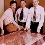
Pictured:  The early Intel management triad.  From left to right:  Andy Grove,  Bob Noyce, Gordon Moore.


Google Trustworthy Response to Product Vulnerabilities Demonstrates Leadership

Google Trustworthy Response to Product Vulnerabilities Demonstrates Leadership
by Matthew Rosenquist on 06-16-2019 at 10:00 am

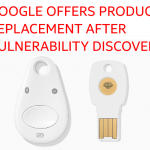
I applaud Google for taking extraordinary steps to protect and service their customers by offering free replacements for the Titan Bluetooth Security Keys. Such product recalls can be expensive, time consuming, and prolong negative stories in the news cycles, yet it is the right thing to do.

Many companies would choose instead to downplay such vulnerabilities, deploy patches which are ineffective or severely impact usability, invest in counter-marketing stories to distract audiences, threaten legal action against researcher to suppress public visibility, or perhaps simply spin the news stores to minimize the brand impact. Actually managing the risks for the benefit of the customer can become a forgotten objective.

The rapid innovation and go-to-market pace of modern electronics precipitates the risks of vulnerabilities. There are practical tradeoffs between security validation and market competitiveness that drive industry best-practices. No matter how diligent the work is to harden products, it is likely that some unknown weaknesses may exist or be discovered.

The moment of truth is when vulnerabilities are discovered. Most big suppliers have product security response or assurance teams. Their policies, decisions, and actions speak volumes about the ethos and responsibility of the organization. Crisis events test the true measure of companies’ commitments and their response exposes the nature of their security organization.

Doing the right thing is tough, but it has its rewards when customer security and experiences are prioritized first. Such ethical responses and transparency builds trust and customer/shareholder loyalty.

I think many companies, especially those with product security assurance/response teams dominated with lawyers and marketing folks, should take note. (hint: lawyers, finance, and marketing people should not lead security). Google is showing what real security leadership looks like: risk professionals working with security engineers and industry experts, making tough decisions in a timely manner, being open and transparent, and doing what is best for the customers regardless of the short-term costs or reputational impact. These are the hallmarks of a good risk mitigation team that is led by security professionals and supported by executive management.

Google responded to the recent Bluetooth vulnerability efficiently and chose to replace the effected products. Such a bold move speaks volumes about how serious, organized, and focused the company is on protecting its customers. Well done.

Google, you have set a high bar. Keep raising the standard and it will become evident which other companies have a marketing-approach to security, allowing consumers to appropriately decide which businesses to trust.

#cybersecurity #technology #trust #vulnerability #infosec


Ecomotion 2019 We are All Jews

Ecomotion 2019 We are All Jews
by Roger C. Lanctot on 06-16-2019 at 8:00 am

While listening to Krista Tippet’s National Public Radio program “On Being” recently I learned of the Hebrew expression familiar to Jews: “tikkun olam.” The expression captures what is described in Wikipedia as an obligation observed by all Jews “to repair the world.”

To be sure, this is an over-simplification of the meaning of the expression. The source and meaning is disputed by some, but the sentiment resonates with Jews and non-Jews alike. In the automotive industry, though, we are all Jews.

Having attended the 7th Annual Ecomotion event in Tel Aviv this week, I can attest to the organic reality of tikkun olam. Hundreds of Israel-based startups are working in the automotive industry and dozens of these companies exhibited at or attended Ecomotion this week in Tel Aviv.

Dozens of technology scouts from transportation companies and venture capitalists from around the world also attended the event. At the core of many of the startup companies is a vision for delivering enhanced automotive safety systems of one sort or another – along with a host of mobility-oriented startups seeking to transform transportation.

All of the executives at these companies working on safety, mobility, cybersecurity, and data analytics can be said to be touched by tikkun olam. In this respect, as executives in the automotive industry, we are all similarly touched. We are all Jews. We share an obligation to fix the world.

We are representatives of an industry that is responsible for 1.3M highway fatalities annually. We are obliged to do something about this.

I moderated a panel discussion at Ecomotion with executives from Vayyar, Arbe Robotics and Magna – all of whom are working on safety systems intended to save lives. I was heartened that each of these panelists recognized their responsibility to take on the task of enhancing automotive safety without hiding behind the favorite industry dodge of blaming drivers.

The Israeli automotive startups attending and exhibiting at Ecomotion reflect the industry-wide effort to reduce or eliminate those 1.3M highway fatalities. The effort embodies an acceptance that car companies and cars can do a better job of helping humans avoid fatal outcomes while driving.

We are all in this together in the automotive industry. While Ecomotion had its greatest success yet with more exhibitors, more attendees and more ideas for solving transportation problems than ever before. Now is the time for action. Now is the time for all of us in the automotive industry to take stock of what we can do to overcome the challenges of cost, performance, and fuel efficiency to design and deliver safer cars.

The ultimate measure of our acceptance of this obligation is to recognize the need to help drivers overcome their weaknesses and limitations. We are bringing a consumer product to market that is killing our customers. We can, we will, we must do better.  We can no longer blame the customer for the shortcomings of our products when we have the necessary technologies within our grasp. Shalom.

EcoMotion Startup Exhibition Map: https://www.ecomotionweek.com/startupexhibition

EcoMotion Booklet 2019: https://docs.wixstatic.com/ugd/58e7a8_7549365fc92640bbb52e306ec83ba5b2.pdf