As semiconductor technology advances into increasingly complex and expensive process nodes, the economic and technical risks associated with ASIC design have grown dramatically. At advanced nodes such as Intel 18A, the cost of a single design error can escalate into tens of millions of dollars, compounded by months of delay. In this environment, embedded FPGA (eFPGA) technology has emerged as a compelling solution, often described as “silicon insurance.” By integrating reconfigurable logic directly into an ASIC, eFPGA enables post-silicon flexibility that can eliminate the need for costly respins. Companies like QuickLogic are at the forefront of this shift, demonstrating that the modest overhead of eFPGA is far outweighed by the financial and strategic benefits it provides.
The fundamental issue with traditional ASIC design lies in its rigidity. Once fabricated, an ASIC is effectively immutable. Any functional bug, evolving standard, or late-stage requirement change necessitates a full respin. This process involves redesigning portions of the chip, regenerating masks, fabricating new wafers, and repeating validation cycles. At leading-edge nodes, mask sets alone can cost tens of millions of dollars, while the full respin cycle can delay product launch by six to twelve months. In fast-moving markets such as artificial intelligence, automotive systems, and data center infrastructure, such delays can result in lost market share that far exceeds the direct engineering costs.
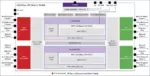
Embedded FPGA addresses this challenge by introducing programmable logic into the ASIC fabric. Unlike fixed-function logic, eFPGA blocks can be reconfigured after fabrication, allowing designers to patch bugs, update algorithms, or adapt to new standards without altering the physical silicon. This capability fundamentally changes the risk profile of chip design. Instead of committing entirely to fixed functionality, designers can reserve a portion of the die for flexibility, effectively hedging against uncertainty. The additional area and power overhead associated with eFPGA becomes a predictable, bounded cost, analogous to an insurance premium while avoiding the potentially catastrophic expense of a respin.
Beyond cost avoidance, eFPGA provides significant advantages in time-to-market. In many applications, being first to market is critical. A respin not only incurs direct costs but also disrupts product timelines, often causing companies to miss key deployment windows. By contrast, eFPGA enables iterative development even after silicon has been deployed. Hardware can evolve alongside software, allowing companies to respond quickly to changing requirements or competitive pressures. This agility is particularly valuable in domains where workloads are not fully defined at design time, such as machine learning accelerators or edge computing platforms.
Historically, one of the main criticisms of FPGA-based approaches has been their impact on power, performance, and area (PPA). However, recent advancements in eFPGA hard IP have significantly narrowed this gap. QuickLogic has been a leader in optimizing eFPGA architectures to reduce overhead while maintaining flexibility. This progress is exemplified by the company’s recent announcement, “QuickLogic Announces Contract for High Density eFPGA Hard IP Optimized for Intel 18A.” This development focuses on architectural enhancements that improve logic density, reduce power consumption, and increase performance, making eFPGA more viable for integration into cutting-edge ASIC designs.
The significance of this announcement extends beyond a single contract. Intel 18A represents one of the most advanced semiconductor nodes, incorporating new transistor architectures and manufacturing techniques that further increase design complexity and cost. By optimizing eFPGA hard IP for such a node, QuickLogic is demonstrating that embedded programmability can coexist with the highest levels of silicon efficiency. Moreover, the architectural improvements developed for this engagement are designed to be extensible across multiple advanced nodes, indicating a broader industry trend toward integrating flexibility directly into the silicon fabric.
This shift reflects a deeper transformation in how hardware is designed and deployed. As systems become more complex and workloads more dynamic, the traditional boundary between hardware and software is blurring. eFPGA enables a more software-like approach to hardware, where functionality can be updated, optimized, and extended over time. This capability is increasingly important for applications that require long lifecycles, such as aerospace, defense, and infrastructure, where replacing hardware is costly or impractical.
Bottom line: eFPGA serves as a form of silicon insurance that fundamentally alters the economics of chip design. By trading a modest increase in area and power for the ability to avoid expensive and time-consuming respins, designers can significantly reduce both financial risk and time-to-market uncertainty. QuickLogic’s work on high-density eFPGA hard IP optimized for Intel 18A underscores the growing maturity of this approach and its relevance at the most advanced process nodes. As the semiconductor industry continues to push the limits of performance and integration, the ability to adapt silicon after fabrication is no longer a luxury, it is a necessity.
Also Read:
Global 2nm Supply Crunch: TSMC Leads as Intel 18A, Samsung, and Rapidus Race to Compete
TSMC vs Intel Foundry vs Samsung Foundry 2026
Intel to Compete with Broadcom and Marvell in the Lucrative ASIC Business