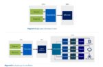
Bronco Webinar 800x100 1

Podcast EP331: Soitec’s Broad Impact on Quantum Computing and More with Dr. Christophe Maleville

Podcast EP331: Soitec’s Broad Impact on Quantum Computing and More with Dr. Christophe Maleville
by Daniel Nenni on 02-13-2026 at 10:00 am

Daniel is joined by Dr. Christophe Maleville, Chief Technology Officer and Senior Executive Vice-President of Soitec’s Innovation. He joined Soitec in 1993 and was a driving force behind the company’s joint research activities with CEA-Leti. For several years, he led new SOI process development, oversaw SOI technology transfer from R&D to production, and managed customer certifications. He also served as vice president, SOI Products Platform at Soitec, working closely with key customers worldwide. He has authored or co-authored more than 30 papers and also holds 30 patents.

In this broad discussion of technology development at Soitec and its impact Dan initially explores with Christophe how Soitec’s work with STMicroelectronics on 28Si FD-SOI substrates is enabling quantum computing development. Christophe also provides details about how Soitec and its work with the semiconductor ecosystem is enabling advances in a broad range of applications including AI, sensing, automotive, and edge AI.

CONTACT SOITEC

The views, thoughts, and opinions expressed in these podcasts belong solely to the speaker, and not to the speaker’s employer, organization, committee or any other group or individual.


TSMC vs Intel Foundry vs Samsung Foundry 2026

TSMC vs Intel Foundry vs Samsung Foundry 2026
by Daniel Nenni on 02-13-2026 at 6:00 am

TSMC vs Intel Foundry vs Samsung Foundry

The global semiconductor industry sits at the foundation of modern technology, powering everything from smartphones and cloud data centers to artificial intelligence, automobiles, and national defense systems. At the center of advanced chip manufacturing are three major players: TSMC, Samsung Foundry, and Intel Foundry. Each represents a distinct manufacturing model and strategic philosophy, and together they form a competitive landscape that is essential for innovation, resilience, and long-term industry health.

TSMC is the undisputed leader in pure-play foundry manufacturing. By focusing exclusively on manufacturing and avoiding competition with its customers in chip design, TSMC has built deep trust with fabless companies such as Nvidia, AMD, Apple, and Qualcomm. This focus has allowed TSMC to lead in process technology, consistently delivering the most advanced nodes such as N5, N3, and the upcoming N2 with strong yields and predictable execution. Its dominance has been especially visible in the AI era, where advanced nodes and packaging technologies like CoWoS have become critical bottlenecks.

Samsung Foundry represents a vertically integrated alternative. As part of Samsung Electronics, it both manufactures chips and designs its own products, including memory, logic, and consumer devices. Samsung has pushed aggressively into leading-edge nodes such as 2nm using gate-all-around (GAA) transistors and continues to invest heavily in advanced packaging and U.S. manufacturing. While Samsung has faced significant challenges in yield consistency compared to TSMC they routinely undercut TSMC wafer pricing. It is hard to figure out the math on that point. Even so, Samsung’s presence provides customers with an important second source at advanced nodes.

Intel Foundry is the most strategically significant entrant into the modern foundry race. Historically a vertically integrated company that designed and manufactured its own chips, Intel is opening its leading edge fabs to external customers while rebuilding its process leadership. Intel’s roadmap includes advanced nodes such as Intel 18A, as well as differentiated capabilities in advanced packaging (EMIB, Foveros) with U.S. based manufacturing. While Intel Foundry is still in the initial stages of winning major external customers, its success would meaningfully rebalance the industry by adding large-scale leading-edge capacity inside the United States.

Competition among these three players is not merely a commercial or political issue, it is structurally critical for the semiconductor ecosystem.

First, competition drives technological progress. Advanced chip manufacturing requires enormous capital investment, deep engineering talent, and long development cycles. Without competitive pressure, there would be less incentive to take risks on new transistor architectures, materials, or manufacturing techniques. The rapid evolution from FinFETs to GAAFET transistors is a direct result of competitive urgency.

Second, competition improves supply-chain resilience. Semiconductors are now a matter of national and economic security. Over-reliance on a single foundry or region increases vulnerability to geopolitical tensions, natural disasters, and capacity shocks. A competitive landscape with strong players in different regions reduces single-point-of-failure risk for governments and industries alike.

Third, customers benefit from choice and leverage. Fabless chip designers depend on foundries not just for wafers, but for co-optimization across design, packaging, and manufacturing. When customers have alternatives, they gain negotiating power on pricing, capacity allocation, and long-term roadmap alignment. This keeps foundries responsive to customer needs rather than dictating terms.

Finally, competition fuels ecosystem growth. Foundries anchor vast networks of equipment suppliers, materials companies, EDA vendors, and OSAT partners. When multiple foundries invest aggressively, the entire ecosystem advances faster, benefiting innovation well beyond any single company.

Bottom line: TSMC, Samsung Foundry, and Intel Foundry are not redundant competitors they are essential counterweights. The semiconductor industry needs all three to succeed, because competition ensures innovation, resilience, and sustainable growth in one of the most strategically important industries in the world, absolutely,

Also Read:

TSMC & GCU Semiconductor Training Program: Preparing Tomorrow’s Workforce

NanoIC Extends Its PDK Portfolio with First A14 Logic and eDRAM Memory PDK

TSMC’s 2026 AZ Exclusive Experience Day: Bridging Careers and Semiconductor Innovation


Silicon Catalyst at the Chiplet Summit: Advancing the Chiplet Economy

Silicon Catalyst at the Chiplet Summit: Advancing the Chiplet Economy
by Daniel Nenni on 02-12-2026 at 10:00 am

Chiplet Summit 2026

The rapid evolution of semiconductor design has elevated chiplets from a niche concept to a foundational strategy for next-generation computing. At the upcoming Chiplet Summit – February 17–19, 2026 Santa Clara Convention Center. Silicon Catalyst will play a central role in shaping this conversation, highlighting how startups, investors, and supply-chain partners can collaborate to unlock value in the emerging chiplet economy.

Through exhibition presence, keynote insights, and a dedicated panel session, Silicon Catalyst  will demonstrate its unique position as an enabler of innovation at the intersection of technology, entrepreneurship, and capital.

Silicon Catalyst’s presence on the exhibition floor underscores its mission as the world’s only accelerator focused exclusively on semiconductor startups. By engaging directly with attendees, Silicon Catalyst will showcase how its comprehensive ecosystem, spanning IP providers, foundries, packaging experts, and venture partners, reduces barriers for early-stage companies seeking to commercialize chiplet-based solutions. In a market where design complexity and manufacturing costs can overwhelm young companies, Silicon Catalyst’s support model offers a critical on-ramp. Leaders from several chiplet companies in Silicon Catalyst’s portfolio will be available for discussions at the show.

A major highlight of the summit will be the presentation by Nick Kepler, Silicon Catalyst COO, on Wednesday, February 18. Nick will emphasize the strategic importance of chiplets in scaling performance, managing cost, and accelerating time to market. By framing chiplets not merely as a technical innovation but as a business enabler, the presentation will reinforce a core theme of the summit: success in the chiplet era depends as much on ecosystem coordination as on engineering excellence.

This theme will come into sharper focus on the Thursday, February 19th panel session at 3pm entitled “Chiplets for Entrepreneurs – Making Money in the Chiplet Game,” hosted by Silicon Catalyst.

The panel session will bring together perspectives from venture capital, the supply chain, and the startup community and includes various presentations and a panel discussion from industry and venture capital executives in the chiplet industry.

The supply-chain perspective will be presented by Qnity (previously DuPont Electronics), highlighting the often underappreciated role of advanced materials, packaging, and manufacturing readiness. As chiplet architectures rely heavily on heterogeneous integration, tight collaboration across the supply chain becomes essential to achieving performance and reliability targets on an industrial scale.

A quick series startup presentations form the core of the session, offering concrete examples of how chiplets are being applied across diverse markets:

  • Athos Silicon covering safety-critical AI compute for the physical world, emphasizing deterministic performance and reduced certification friction for autonomy.
  • CrossFire Technologies addressing one of AI’s most pressing challenges, the compute-to-memory bottleneck, through its patented Bridgelet™ products.
  • HEPT Lab will illustrate the power of heterogeneous integration with its multi-chiplet 3D image sensor combining silicon photonics, CMOS, and InP technologies into a single package.
  • Quadric AI will showcase its fully programmable, chiplet-ready AI inference IP, targeting generative AI and autonomous driving.

The concluding panel discussion, featuring leaders from startups, the investment community, and the supply chain, is targeted at reinforcing the idea that chiplets are not a silver bullet but a powerful tool when paired with the right ecosystem support. The key is that technical innovation, manufacturability, and business strategy must evolve together.

Bottom line: Silicon Catalyst’s leadership at the Chiplet Summit highlights its pivotal role in transforming chiplets from promising technology into viable businesses. By convening investors, suppliers, and entrepreneurs under a shared vision, Silicon Catalyst is helping to define how value is created, and captured, in the chiplet era, making it a cornerstone of the semiconductor industry’s next growth chapter.

Note: Silicon Catalyst has arranged a special Chiplet Summit registration discount code that you can use at checkout:  CS26SICA

REGISTER NOW

Also Read:

Silicon Catalyst: Searching for the Next Great Start-up

Revitalizing Semiconductor StartUps

Silicon Catalyst on the Road to $1 Trillion Industry


Giving AI Agents Access to a Compiled Design and Verification Database

Giving AI Agents Access to a Compiled Design and Verification Database
by Tom Anderson on 02-12-2026 at 8:00 am

SemiWiki Snapshot

A few weeks ago, I had the chance to work with AMIQ EDA as they introduced a new product: DVT MCP Server. I was quite intrigued by the role it will play in AI-assisted chip design and verification, so I wanted to learn more. I spoke with Gabriel Busuioc, the AI Assistant team leader at AMIQ EDA, to understand more about the product and how their users will benefit from it.

Busu, it is great to talk with you. What is your role?

I have worked at AMIQ EDA for almost five years now. I started as an intern and joined full-time after I earned an MS in Advanced Software Services from the Politehnica University of Bucharest. I’ve worked on several very interesting projects, adding new features to our existing products as well as developing this new product.

What was the motivation for DVT MCP Server?

As you know, we provide integrated development environments (IDEs) and related tools for hardware design and verification. We support a wide range of languages, all of which we compile and elaborate. We connect together the code from hundreds or thousands of files into a single internal database of the complete hierarchical design and verification environment. That database gives us the ability to enable very smart editing, automated analysis and linting, debugging, documentation generation, and more.

This compiled database is internal to your Design and Verification Tools (DVT) products, correct?

Yes, and that’s where DVT MCP Server comes in. We started to wonder whether other tools, specifically AI agents, could benefit if they had access to project information within our internal database. It turned out that there is an open industry standard called Model Context Protocol (MCP) that serves exactly this purpose. It’s designed to connect AI agents to external data and applications. The goal is to make AI results more accurate by providing access to specialized or application-specific knowledge that was not learned through general training.

That sounds like the sort of knowledge in your database.

Exactly. We have detailed knowledge of design and verification languages plus of course the project-specific knowledge of the design and verification environment. DVT MCP Server allows all sorts of other applications to benefit from our knowledge and invoke our analysis engines.

Can you please give an example of how this might work?

Many engineers are experimenting with using AI to generate code, including for design and verification environments. They’re finding that AI agents are more effective with general-purpose languages than domain-specific languages. Limited training data and lack of context means that AI may hallucinate or generate incorrect code. DVT MCP Server provides quick, compiler-backed feedback to ground AI reasoning in accurate language semantics and their project context while detecting any errors in generated code.

So the benefit to users is better design and verification code?

Yes, that is what our users are reporting. If an AI agent makes a subtle language error, or incorrectly references part of the design or testbench, DVT MCP Server catches that and reports it back to the agent. Users don’t need to pay attention to errors that happen internally; all they see is correctly generated code. AI agents can understand, generate, modify, debug, and correct code for real-world design and verification projects efficiently and accurately. This is simply not possible using only generic training data.

What else should we know?

DVT MCP Server supports Verilog, SystemVerilog, VHDL, and the e language, so it covers the most widely used languages for chip development. It can run within DVT IDE to provide live project context to interactive AI assistants, or operate in batch mode to support fleets of AI agents in automated workflows.

Is this related to AI Assistant that you introduced in late 2024?

You can think of them as complementary. AI Assistant runs within our products, enabling users to generate, modify, and understand code more easily. It relies on our internal design and verification database. DVT MCP Server provides external access to information in this same database for other tools to yield better results.

Is there anything new with AI Assistant?

Yes. We originally introduced this feature for DVT IDE, but have now integrated it with all our products. For example, it enables Verissimo SystemVerilog Linter to better explain and auto-correct linting failures in design and verification code. AI Assistant also helps Specador Documentation Generator produce description comments, for example to fully document a module or entity, including all ports and signals. Moreover, we’ve enhanced AI Assistant within DVT IDE with a new Agentic profile that enables the connected LLM to autonomously get project information and do file edits end-to-end. All the users have to do is specify their requests in plain, natural language.

How can our readers learn more?

You can start with our product page, and then request a demo or an evaluation license. You can also meet with members of our team in person at DVCon U.S. in Santa Clara March 2-5, where we will be exhibiting at Booth 204. We hope to talk with you there or online.

Busu, thank you very much for your time. AI and AMIQ EDA are two great topics to discuss.

I agree, and I think they’re even more exciting when combined. Thank you, Tom.

Also Read:

2026 Outlook with Cristian Amitroaie, Founder and CEO of AMIQ EDA

Runtime Elaboration of UVM Verification Code

Better Automatic Generation of Documentation from RTL Code


How Memory Technology Is Powering the Next Era of Compute

How Memory Technology Is Powering the Next Era of Compute
by Kalar Rajendiran on 02-11-2026 at 10:00 am

How AI is Shaping the Memory Market Title Slide

For more than a decade, progress in artificial intelligence has been framed almost entirely through the lens of compute. Faster GPUs, denser accelerators, and higher TOPS defined each new generation. But as generative and agentic AI enter their next phase, that framing is no longer sufficient. The most advanced AI systems today are not constrained by arithmetic throughput. They are constrained by memory.

That reality was the central theme of “How Memory Technology Is Powering the Next Era of Compute,” a panel session featuring Rambus participants Steven Woo, John Eble, and Nidish Kamath, moderated by Timothy Messegee. Timothy is Senior Director, Solutions Marketing; Steven is a Fellow and Distinguished Inventor; John is Vice President, Product Marketing for Memory Interface Chips; and Nidish Kamath, is Director, Product Management, Memory Controller IP.

The discussion revealed how modern AI workloads are placing unprecedented demands across the entire memory hierarchy, forcing fundamental changes in system architecture, power delivery, and reliability strategies.

When AI Models Outgrow the Memory Hierarchy

The defining characteristics of today’s AI models include exploding parameter counts, longer context windows, persistent reasoning, and simultaneous multi-user inference. All these characteristics translate directly into dramatically higher memory demands. AI systems now need to move, store, and retain far more data than previous generations of workloads, often for extended periods of time.

At the same time, scaling limits at the lowest levels of the memory hierarchy are becoming increasingly visible. SRAM no longer scales economically or densely enough to keep pace with AI’s appetite for on-chip data. As a result, pressure shifts upward into DRAM, which must now deliver both higher bandwidth and greater capacity. The traditional memory hierarchy, designed for more balanced and predictable workloads, is struggling to adapt to this imbalance.

Architecture Steps In Where Physics Pushes Back

In server environments, the constraints are especially acute. CPUs can only support a limited number of memory channels due to pin count, packaging, and system form-factor limitations. Simply adding more memory channels is not practical, yet AI workloads demand more bandwidth than ever.

This is where architectural innovations such as MRDIMM, or Multiplexed Rank DIMM, become critical. MRDIMM technology uses on-module logic to multiplex parallel memory ranks into a single CPU channel, effectively doubling usable bandwidth without requiring additional pins or channels. Rather than relying solely on faster DRAM devices, MRDIMM demonstrates how intelligent system design can extend performance beyond traditional physical limits.

Telemetry: From Debug Tool to Performance Enabler

Another important shift highlighted during the panel is the growing role of telemetry and observability. In earlier generations, memory subsystems were largely static, configured once and rarely revisited. That approach no longer works in AI systems, where workloads evolve rapidly and performance requirements shift continuously.

Modern memory controllers now provide detailed visibility into internal behavior, enabling real-time tuning and long-term optimization. This level of observability allows systems to adapt as AI models change, sustaining performance and efficiency rather than allowing them to degrade over time. In this context, telemetry is no longer just a debugging aid, it has actually become a core enabler of AI performance.

Reliability Moves to the Center of AI Infrastructure

As AI deployments scale, reliability has emerged as a defining constraint. Memory-related errors already contribute to significant system downtime in large data centers, driving costly overprovisioning to maintain service levels. For AI workloads, where training and inference cycles are both expensive and time-sensitive, an overprovisioning approach is unsustainable.

The panel emphasized that reliability, availability, and serviceability features must now be designed into memory systems from the outset. Advanced error correction, cyclic redundancy checks, retry mechanisms, and fault isolation are becoming essential for sustaining AI uptime. Performance without reliability is no longer acceptable in large-scale AI infrastructure.

Memory Technologies Begin to Converge

One of the most striking themes to emerge from the discussion is the blurring of traditional memory boundaries. Technologies once confined to specific markets are now being reevaluated through the lens of AI workloads.

GDDR7, historically associated with graphics, is increasingly attractive for edge inference. Its use of PAM3 signaling delivers exceptional bandwidth while controlling pin count, and built-in retry mechanisms improve robustness in environments where reliability matters. Meanwhile, LPDDR5X and LPDDR6, long optimized for mobile devices, now offer bandwidth comparable to DDR5 while maintaining superior power efficiency. New modular formats such as LPCAMM2 further extend LPDDR’s reach by combining proximity to the processor with serviceability.

As a result, memory selection is becoming less about market segmentation and more about workload fit.

Power Becomes the Dominant Design Constraint

As AI systems grow denser and more powerful, power delivery has become one of the most difficult challenges facing system architects. Future AI data centers are being designed around megawatt-class racks, driven by high-bandwidth memory, dense accelerators, and massive data movement.

A growing share of total system energy is now consumed not by computation, but by moving data between components. To manage this, architectures are shifting toward higher-voltage, lower-current delivery, with power management integrated directly onto memory modules through PMICs. Even fractional improvements in efficiency can translate into enormous savings at scale.

These power densities also drive changes in cooling strategies. Liquid cooling is rapidly becoming standard in AI systems, reshaping server design and data center infrastructure. Memory, once a relatively passive consideration, is now deeply intertwined with power and thermal architecture.

Chasing the “Best of Both Worlds”

Looking ahead, the panel pointed toward a future in which memory technologies blend strengths that were once considered mutually exclusive. The goal is to combine the bandwidth and power efficiency of mobile-class memory with the reliability, security, and resilience traditionally associated with server-class systems.

This direction opens the door to innovations such as processing-in-memory, inline memory encryption, and new reliability frameworks tailored specifically for AI workloads. As systems evolve toward agentic and autonomous behavior, memory will play a central role in enabling not just performance and scale, but trust, privacy, and long-term stability.

A New Mandate for Memory

The AI revolution has fundamentally changed what is expected from memory systems. Faster alone is no longer sufficient. Memory must now be closer to compute, more efficient, deeply observable, highly reliable, and inherently secure.

AI did not simply expose the limits of the old memory playbook. It is driving its rewrite.

You can watch the entire Rambus panel session here.

Also Read:

Chiplets Reach an Architectural Turning Point at Chiplet Summit 2026

Gate-All-Around (GAA) Technology for Sustainable AI

VSORA Board Chair Sandra Rivera on Solutions for AI Inference and LLM Processing


Semidynamics Unveils 3nm AI Inference Silicon and Full-Stack Systems

Semidynamics Unveils 3nm AI Inference Silicon and Full-Stack Systems
by Daniel Nenni on 02-11-2026 at 8:00 am

Semidynamics Unveils TSMC N3 AI Inference Silicon

Semidynamics has taken a significant step forward in the race to build next-generation AI infrastructure with the unveiling of its 3nm AI inference silicon and a vertically integrated, full-stack systems strategy. Announced in February 2026, the development marks the company’s evolution from an advanced architecture specialist into a full-stack AI platform provider, delivering not only chips but also boards and rack-scale systems designed for demanding data center inference workloads. At a time when AI performance is increasingly constrained by memory efficiency and system integration rather than raw compute alone, Semidynamics’ approach reflects a clear shift toward system-level optimization.

Central to this announcement is the company’s successful 3nm tape-out with TSMC, achieved in December 2025. Fabricated using one of TSMC’s most advanced process technologies, this milestone validates Semidynamics’ ability to execute at the leading edge of semiconductor manufacturing. Tape-out at 3nm is not only a technical achievement but also a signal of silicon readiness, placing Semidynamics among a small group of companies capable of translating complex AI architectures into manufacturable, production-grade designs on the world’s most advanced nodes.

While the use of TSMC’s 3nm technology provides density, performance, and power-efficiency advantages, Semidynamics emphasizes that process scaling alone is not sufficient to meet the needs of modern AI inference. As AI models continue to grow in size and concurrency requirements increase, memory bandwidth and data movement have emerged as the dominant performance bottlenecks. This so-called “memory wall” limits the real-world gains achievable by compute-centric designs and drives up system cost and power consumption.

To address this challenge, Semidynamics has developed a new memory subsystem that rethinks data flow and memory access from first principles. Rather than relying heavily on scarce and expensive high-end memory components, the architecture optimizes how data is moved, reused, and accessed across the system. This enables large inference models to operate more efficiently, supports high-concurrency workloads, and reduces total cost of ownership for data center operators. The result is an architecture designed not just for peak performance, but for sustained, scalable inference in real deployment environments.

Building on this silicon foundation, Semidynamics is expanding into a full-stack AI infrastructure model. The company plans to deliver tightly integrated boards and rack-level systems based on its 3nm inference silicon, ensuring that architectural benefits at the chip level translate directly into system-level gains. This vertical integration is increasingly important in modern AI data centers, where performance, power efficiency, and scalability depend on how well accelerators, interconnects, and system software are co-designed.

By offering a complete stack (chips, boards, and racks), Semidynamics aims to reduce integration complexity for customers and provide predictable performance across multi-accelerator configurations. This approach contrasts with more fragmented models, where silicon vendors leave system optimization largely to OEMs and hyperscalers. For inference-heavy workloads that demand high throughput, low latency, and energy efficiency, such end-to-end optimization can be a decisive advantage.

Company leadership has positioned the 3nm tape-out with TSMC as a critical validation point in a broader, multi-stage roadmap. The goal is not simply to demonstrate advanced silicon, but to deliver production-ready AI inference platforms capable of operating at scale in next-generation data centers. This long-term perspective reflects Semidynamics’ architectural heritage and its focus on building durable platforms rather than one-off accelerators.

The announcement also carries strategic significance beyond technology. As a European-headquartered company designing advanced AI silicon manufactured at TSMC, Semidynamics represents a bridge between global manufacturing leadership and regional architectural innovation. This positioning aligns with broader efforts to strengthen Europe’s role in advanced computing while leveraging best-in-class foundry capabilities.

Bottom line: Unveiling its 3nm AI inference silicon and full-stack systems strategy, Semidynamics is addressing the realities of the current AI landscape. Performance gains are increasingly determined by memory efficiency and system integration, not just transistor counts. By combining an advanced 3nm implementation at TSMC with a memory-centric architecture and vertically integrated systems, Semidynamics is positioning itself as a differentiated player in AI inference infrastructure—one focused on scalable, efficient, and deployable solutions for the data centers of the future.

CONTACT SEMIDYNAMICS

Also Read:

2026 Outlook with Volker Politz of Semidynamics

Semidynamics Inferencing Tools: Revolutionizing AI Deployment on Cervell NPU

From All-in-One IP to Cervell™: How Semidynamics Reimagined AI Compute with RISC-V


Watch Live Agentic Software Debug

Watch Live Agentic Software Debug
by Bernard Murphy on 02-11-2026 at 6:00 am

agentic debug cppcon

Many moons ago in the Innovation series we explored techniques like spectrum analysis to root-cause bugs. While these methods provide some value they don’t get as close as we would like to isolating a root-cause. In hindsight given what we know about the complexity of conventional debug it is unsurprising that we can’t root-cause in one shot. Hence the rise of agentic debug solutions from companies like ChipAgents and ChipStack. Agentic systems can reason through a root cause analysis in multiple steps just as we do in human-based analysis. Following is a very intriguing parallel from our sister field (software debug) posted as a YouTube session from the C++ conference.

(Image courtesy of Cppcon)

Background and bugs

This event was a joint presentation between UnDo.io (who provide time-travel debugging for C++ and Java, think something like gdb with full context replay) and Anthropic. Their goal was to explore live (not a canned demo) what agentic debugging would look like. Gutsy move because the reality was messy though still very informative. They test on a couple of cases in parallel: A segfault in the Python interpreter and unexpected behaviors (which prove not to be bugs) in Doom.

The Python bug should attract the interest of hardware designers: effectively a cache coherency issue in software. The code caches pointers to objects allocated in memory and entries in the cache can be tested without incrementing reference counts for those objects. The coherency risk is that a referenced object may be freed without clearing the cache reference, a worthy test for the value of agentic debugging. The Doom exploration is primarily interesting for how it influences the debugging process in localizing a behavior within a playback to get close to whatever triggered that behavior. This case may be even more interesting for hardware debug, where unexpected behavior is much more likely than anything comparable to a crash.

My takeaways from the demo

The Python debug demo is, as far as I can tell, hands-free apart from the initial setup. Analysis starts with the crash and iterates backwards and between multiple types of agents, trying different hypotheses, testing with different techniques to eliminate possibilities. UnDo added an adversarial “bug diagnosis validator” agent (Claude Code) provides support for this). As agentic analysis progresses, discoveries start to converge towards the right area ultimately getting get pretty darn close to the root cause.

As expected, Claude builds a ToDo list of tasks it believes it needs to perform to work towards a goal (e.g. find when the second zombie was killed in the Doom debug, see below), and checks these off as it progresses. An interesting revelation is that it apparently can lose the plot periodically, at which point it needs to be reminded to revisit the list. This didn’t seem to happen in this Python case.

The Doom analysis is more collaborative, I imagine because they don’t have a bug to target. Instead, they are trying to understand unexpected”behaviors. For example, why did the player get stuck in the map room after killing the second Zombie? Here the demo guy asked, “when was the second zombie killed during this playthrough (recorded playback)?” Claude got him to this point, from which he could ask it to drill down further. Note the value of being able to use a high level reference (second zombie) in prompting next steps.

The demo often ran into system problems (“repeated server overload with “Opus model” – Opus is Claude’s model optimized for coding) which seem to reflect server busy problems on the Claude side. These issues are now apparently fixed (or at least improved) – this demo was running with a pre-release of the Claude Code API.

There was question from the audience about token costs. The UnDo speaker suggested single-digit dollars for the Doom example (56k LOC), much higher costs  ($$ numbers not cited) to track down the Python interpreter bug mentioned earlier (350k C LOC, 800k Python LOC).

Long video (about an hour) but well worth watching all the way through for the insights it provides. You can find the video HERE.

Also Read:

Why PDF Solutions Is Positioning Itself at the Center of the Semiconductor Ecosystem

Gate-All-Around (GAA) Technology for Sustainable AI

Beyond Transformers. Physics-Centric Machine Learning for Analog


Accellera Strengthens Industry Collaboration and Standards Leadership at DVCon U.S. 2026

Accellera Strengthens Industry Collaboration and Standards Leadership at DVCon U.S. 2026
by Daniel Nenni on 02-10-2026 at 10:00 am

DVCON 2026

At DVCon U.S. 2026, Accellera Systems Initiative reinforces its central role in shaping the future of electronic design and verification through a focused program of workshops, tutorials, and community engagement. As system complexity continues to rise across AI, automotive, HPC, and communications markets, the need for robust, interoperable standards has become more urgent. Accellera’s presence at DVCon highlights how standards development is evolving to address verification scalability, system-level modeling, and IP reuse in increasingly heterogeneous designs.

We have been working with Accellera since the early days of SemiWiki when our membership was in the thousands. Now our members are in the hundreds of thousands and it really has been a pleasure working with them.

A central theme of Accellera’s program is raising the level of abstraction in design and verification. The workshop on Portable Stimulus Standard (PSS) exemplifies this shift. As SoC verification expands beyond simulation into emulation, FPGA prototyping, and post-silicon validation, traditional testbench-centric approaches struggle to scale. PSS addresses this by allowing engineers to model verification intent at the scenario level, enabling automated generation of tests that can be reused across platforms. By focusing on practical adoption patterns, Accellera positions PSS not as a theoretical construct, but as a pragmatic solution for revitalizing legacy flows and improving coverage in real-world environments

Accellera-Sponsored Events:

Monday, March 2:
Portable Stimulus Modeling Patterns (Practical Tips for Adopting PSS)
9:00-10:30am, Grand Ballroom D

SystemC – What’s New? What’s Next?
11:00am-12:30pm, Grand Ballroom D

Thursday, March 5:
Breakthrough in CDC-RDC Verification Defining a Standard for Interoperable Abstract Model
9:00am-12:30pm, Grand Ballroom D:

IP-XACT Demystified: An In-Depth Training on the IEEE 1685-2022 IP-XACT Standard
1:30-3:00pm, Grand Ballroom D

Another major pillar of Accellera’s DVCon engagement is the continued evolution of SystemC, long regarded as foundational for system-level modeling and virtual platforms. While SystemC has matured significantly, new architectural demands such as chiplet-based designs, software-defined hardware, and large-scale virtual prototyping require renewed attention to interoperability and tooling. The session outlining updates from IEEE 1666-2023, along with progress on the SystemC CCI reflects Accellera’s recognition that standards must evolve in lockstep with industry practice. Lessons drawn from widely adopted open-source frameworks such as QEMU further underscore the importance of learning from production-proven ecosystems rather than relying solely on academic or vendor-specific approaches

Verification correctness and predictability across complex clocking environments is another area where Accellera is driving standardization. The CDC-RDC tutorial introduces efforts by the Clock Domain Crossing Working Group to define a standardized abstract model using IP-XACT and TCL. CDC and RDC issues remain among the most subtle and costly classes of silicon bugs, particularly in large SoCs integrating third-party IP. By working toward a portable, interoperable CDC-RDC model, Accellera aims to reduce tool fragmentation and enable consistent verification flows across vendors, a long-standing industry challenge

The focus on IP-XACT (IEEE 1685-2022) further emphasizes Accellera’s commitment to automation and reuse. As SoC integration teams grapple with exploding register maps, memory hierarchies, and software dependencies, spreadsheet-based approaches have become untenable. The updated IP-XACT standard provides a vendor-neutral framework for capturing IP metadata in a structured, machine-readable form. Accellera’s in-depth training session reflects growing recognition that design, verification, and software teams must operate from a single source of truth to avoid costly integration errors and delays

Beyond the technical content, Accellera’s DVCon activities highlight the importance of community-driven standards development. The Birds-of-a-Feather discussion following the SystemC session and the evening reception are not peripheral events; they are integral to how consensus is built and future directions are shaped. In an era where proprietary solutions can fragment ecosystems, Accellera’s neutral, not-for-profit model remains a critical mechanism for aligning semiconductor companies, IP providers, and EDA vendors around shared technical foundations.

Overall, Accellera’s presence at DVCon U.S. 2026 reflects a broader industry transition. As scaling challenges shift from pure transistor density to system integration, verification productivity, and software alignment, standards are no longer optional—they are strategic infrastructure. Through its workshops, tutorials, and collaborative forums, Accellera continues to position itself as a catalyst for that infrastructure, ensuring the electronics industry can move forward with greater confidence, interoperability, and efficiency.

For a complete program schedule, including exhibition hours, visit the DVCon U.S. 2026 website.

Registration is open. Registration for the keynotes, panel, and exhibits is free.

Also Read:

Podcast EP330: An Overview of DVCon U.S. 2026 with Xiaolin Chen

Boosting SoC Design Productivity with IP-XACT

Podcast EP310: On Overview of the Upcoming DVCon Europe Conference and Exhibition with Dr. Mark Burton


Ceva Wi-Fi 6 and Bluetooth IPs Power Renesas’ First Combo MCUs for IoT and Connected Home

Ceva Wi-Fi 6 and Bluetooth IPs Power Renesas’ First Combo MCUs for IoT and Connected Home
by Daniel Nenni on 02-10-2026 at 8:00 am

unnamed (2)

The rapid expansion of IoT, smart home, and industrial automation markets is reshaping how connectivity is designed into embedded systems. Developers increasingly require highly integrated wireless solutions that deliver strong performance, ultra-low power consumption, and design flexibility, while also shortening development cycles and reducing system cost. Addressing these needs, Ceva, Inc. (NASDAQ: CEVA), the leading licensor of silicon and software IP for the Smart Edge, announced that Renesas Electronics Corporation has integrated Ceva-Waves™ Wi-Fi 6 and Bluetooth® Low Energy (LE) IPs into its newly launched RA6W1 and RA6W2 microcontrollers (MCUs), marking Renesas’ first combo wireless MCU offerings.

Renesas’ RA6W1 and RA6W2 MCUs are designed to support a broad range of connected applications, including smart home devices, industrial IoT, consumer electronics, and building automation. The RA6W1 integrates dual-band Wi-Fi 6, while the RA6W2 combines Wi-Fi 6 and Bluetooth LE into a single MCU platform. By leveraging Ceva-Waves connectivity IPs, Renesas enables developers to choose between standalone Wi-Fi designs, Wi-Fi/Bluetooth LE combo solutions, or fully integrated wireless modules, depending on performance, cost, and power requirements.

This flexibility is increasingly critical as IoT devices diversify across use cases, from battery-powered sensors and smart appliances to industrial controllers and gateways. The Ceva-powered RA6W1 and RA6W2 solutions simplify system architecture by reducing the need for external connectivity components, lowering bill-of-materials costs, and streamlining RF and software integration. At the same time, they offer both hosted and hostless implementation options, allowing customers to tailor system partitioning and optimize overall efficiency.

Power efficiency remains a key differentiator in IoT and connected home markets, where battery life and thermal constraints directly impact product usability and lifetime. Ceva-Waves Wi-Fi 6 and Bluetooth LE IPs are optimized for low-power operation without compromising throughput, reliability, or interoperability. Wi-Fi 6 brings benefits such as improved spectral efficiency, reduced latency, and better performance in dense environments, while Bluetooth LE provides energy-efficient short-range connectivity for device provisioning, control, and data exchange. Together, these technologies enable always-connected devices that operate reliably within strict power budgets

“Connected devices are advancing at an unprecedented pace, opening new opportunities in IoT and industrial applications,” said Chandana Pairla, Vice President of Connectivity at Renesas. “By incorporating Ceva’s Wi-Fi and Bluetooth LE IPs into our MCUs, we are delivering system-level connectivity that combines high performance with exceptional energy efficiency. This integration helps customers reduce design complexity, extend battery life, and accelerate time to market in smart home and industrial automation applications.”

From Ceva’s perspective, the collaboration highlights the growing role of licensable connectivity IP in enabling scalable, standards-compliant wireless solutions across a wide range of MCU and SoC designs. “Our unique connectivity IP portfolio delivers the performance and efficiency needed to bring next-generation wireless features into MCUs,” said Tal Shalev, Vice President and General Manager of the Wireless IoT Business Unit at Ceva.

“This collaboration with Renesas reinforces our role as a trusted partner, enabling faster IoT innovation and empowering developers to expand what’s possible at the smart edge.”

Ceva-Waves is a comprehensive portfolio of wireless connectivity IPs supporting Wi-Fi 6 and Wi-Fi 7, Bluetooth LE and Dual Mode, IEEE 802.15.4, Ultra-Wideband (UWB), and turnkey multiprotocol platforms that also support Thread, Zigbee, and Matter. With proven hardware implementations and complete software stacks, Ceva-Waves enables faster integration, reduced risk, and shorter time to market for MCU and SoC developers targeting next-generation IoT and connected home devices.

Bottom line: By combining Renesas’ robust MCU platforms with Ceva’s industry-proven connectivity IPs, the RA6W1 and RA6W2 MCUs set a new benchmark for flexible, power-efficient wireless integration helping developers meet the evolving demands of the connected world while accelerating innovation at the smart edge.

Also Read:

Ceva-XC21 Crowned “Best IP/Processor of the Year”

United Micro Technology and Ceva Collaborate for 5G RedCap SoC and Why it Matters

Ceva Unleashes Wi-Fi 7 Pulse: Awakening Instant AI Brains in IoT and Physical Robots


Why PDF Solutions Is Positioning Itself at the Center of the Semiconductor Ecosystem

Why PDF Solutions Is Positioning Itself at the Center of the Semiconductor Ecosystem
by Kalar Rajendiran on 02-10-2026 at 6:00 am

PDF Solutions Thank You

The semiconductor industry is on track to exceed one trillion dollars in annual revenue by the end of the decade, propelled by AI, advanced computing, and edge applications. Yet beneath this growth lies a structural shift. Manufacturing complexity is rising faster than the industry’s ability to manage it. As architectures move deeper into 3D, production disperses globally, and product cycles compress, scale alone is no longer a differentiator. Operational coherence is.

In this environment, competitive advantage increasingly depends on how effectively organizations can learn, decide, and act across organizational boundaries. PDF Solutions’ 2026 priorities reflect a clear recognition of this shift: the company is evolving from a best-in-class analytics provider into a coordination and orchestration platform positioned at the center of the semiconductor ecosystem.

The following analysis reflects PDF Solutions’ stated priorities, positioning, and marketing opportunities based on its most recent Analyst Day presentation.

Manufacturing Analytics as Infrastructure, Not Just Tools

For decades, manufacturing analytics functioned as an overlay. Though powerful, it was disconnected from direct execution. PDF is reframing analytics as infrastructure: a shared data backbone that spans characterization, process development, high-volume manufacturing, test, and assembly. This distinction is critical as data volumes explode and process interactions become increasingly nonlinear.

By standardizing how data is ingested, contextualized, and analyzed across domains, PDF’s Exensio platform reduces reliance on custom integrations and tribal knowledge. The result is not simply better visibility, but a common analytical language that enables faster root-cause analysis, more consistent decision-making, and shared accountability across teams and partners. Additionally, it is clear that valuable, trusted, production-ready applications of AI in an industrial context need to be anchored on that type of robust, scalable, and secure data platform. PDF Solutions aims to be the platform enabling the scaling of AI across the semiconductor ecosystem.

Why Analytics Alone Is No Longer Enough

Insight without execution has diminishing value in a distributed manufacturing environment. Analytics can explain what happened and why, but as fabs scale and supply chains fragment, decision latency becomes as costly as yield loss. The next bottleneck is no longer diagnosis but orchestrated execution.

PDF’s strategy reflects this reality. Rather than stopping at insight, the platform embeds analytics directly into manufacturing workflows, ensuring that conclusions translate into aligned action across fabs, test operations, and external partners. This shift moves analytics from advisory to operationally critical.

From Insight to Orchestration

Orchestration is where PDF’s positioning becomes distinctly strategic. Orchestration answers not just “what should happen next,” but also ensures that it actually does. By connecting data, decisions, and actions, PDF enables coordinated responses to yield excursions, prioritizes engineering resources, and synchronizes operations across organizational boundaries.

This evolution is visible in Exensio’s role as an operating layer rather than a standalone analysis environment. It is further reinforced by secureWISE, which extends orchestration beyond the enterprise, enabling standardized, governed data exchange across the broader semiconductor ecosystem. Together, these capabilities position PDF not as another analytics vendor, but as the system that aligns learning and execution at scale.

Orchestration as a Strategic Risk Reducer

As semiconductor manufacturing becomes more globally distributed, coordination failures carry outsized consequences, from delayed ramps to systemic yield losses. Orchestration directly addresses this growing strategic risk. Standardized data exchange and shared workflows enable faster diagnosis, tighter alignment, and more resilient operations across regions and partners.

This elevates platforms like PDF’s from operational tools to strategic assets. The ability to coordinate learning and execution across a fragmented ecosystem becomes as important to resilience as it is to performance.

Secure Data Exchange in a Distributed Ecosystem

Modern semiconductor manufacturing is inherently cross-enterprise. Foundries, OSATs, equipment suppliers, and customers must collaborate without compromising security or IP. PDF’s secureWISE initiative reframes this challenge as a network and standardization problem rather than a series of custom integrations.

By enabling secure, governed data exchange across organizations, secureWISE supports functional consolidation without ownership consolidation. Participants remain independent, but coordinate through shared data models and workflows. As supply chains become more dynamic and geopolitical risk increases, this capability shifts from a differentiator to a requirement.

AI in Manufacturing: Discipline Over Hype

AI is a core pillar of PDF’s platform strategy, but its positioning is deliberately pragmatic. Manufacturing AI operates under constraints that differ sharply from consumer or enterprise applications: low tolerance for error, high accountability, and the need for explainability.

PDF embeds AI within governed analytics environments where models augment engineering judgment rather than replace it. The focus is on productivity, yield improvement, and cycle-time reduction rather than experimentation for its own sake. AI becomes an operational lever, not a speculative bet.

Platform Economics and Financial Leverage

PDF’s technical strategy is reinforced by a clear economic model. The company continues to expand recurring and usage-based revenue streams through subscriptions, cloud deployment, and volume-linked offerings such as secureWISE, Cimetrix, and gainshare. Analytics revenue is growing faster than total revenue, margins are expanding, and backlog growth outpaces the top line, all clear signals of increasing platform maturity.

Importantly, these offerings are becoming embedded deeper into customer operations, positioning PDF’s platform as production infrastructure rather than discretionary IT. This alignment between customer success and revenue growth strengthens financial leverage and durability.

Platform Economics and the Valuation Question: Why This Moment Matters

Despite this evolution, market perception has lagged execution. PDF is still often viewed as a niche analytics specialist rather than a system-level orchestrator. Closing this perception gap represents one of the company’s largest marketing opportunities. The company is working hard trying to change that perception with for example the recent SEMICON WEST keynote given by John Kibarian, PDF Solutions’ CEO emphasizing the need and opportunity for more AI driven collaboration across the semiconductor industry.

The semiconductor industry is approaching an inflection point. Fragmentation, rising complexity, and accelerating demand cycles are colliding with higher capital intensity and tighter talent constraints. Large-scale consolidation is neither practical nor desirable. The more likely outcome is convergence around a small number of coordination platforms that allow diverse ecosystems to function as coherent systems.

PDF Solutions is positioning itself squarely in that role. As a neutral, vendor-agnostic coordination layer, it can benefit from ecosystem fragmentation rather than fight it. When more tools and partners rely on the same platform to share data and coordinate work, the platform naturally becomes more valuable and harder to walk away from. Its future value will be defined less by individual products and more by how deeply it becomes embedded in industry operations.

In an environment where coordination is the new constraint, platforms that enable shared learning and aligned execution may prove to be among the most strategically valuable assets in semiconductor manufacturing.

Learn more at www.pdf.com and here.

Also Read:

Manufacturing Is Strategy: Leadership Lessons from the Semiconductor Front Lines

PDF Solutions’ AI-Driven Collaboration & Smarter Decisions

PDF Solutions Charts a Course for the Future at Its User Conference and Analyst Day