Synopsys IP Designs Edge AI 800x100

UCIe 3.0: Doubling Bandwidth and Deepening Manageability for the Chiplet Era

UCIe 3.0: Doubling Bandwidth and Deepening Manageability for the Chiplet Era
by Daniel Nenni on 08-05-2025 at 10:00 am

Chiplet SemiWiki UCIe

The Universal Chiplet Interconnect Express (UCIe) 3.0 specification marks a decisive step in the industry’s shift from monolithic SoCs to modular, multi-die systems. Released on August 5, 2025, the new standard doubles peak link speed from 32 GT/s in UCIe 2.0 to 48 and 64 GT/s while adding a suite of manageability and efficiency features designed to make chiplet-based systems faster to initialize, more resilient in operation, and easier to scale. The focus is clear: deliver more bandwidth density at lower power to feed AI and other data-hungry workloads without sacrificing interoperability.

What distinguishes UCIe 3.0 is the way raw performance is paired with lifecycle controls. On the physical layer and link management fronts, the spec introduces runtime recalibration so links can retune on the fly by reusing initialization states, cutting the penalty traditionally paid when conditions change. An extended sideband channel—now reaching up to 100 mm—expands how far control signals can travel across a package, enabling more flexible topologies for large, heterogeneous SiPs. Together, these advances let designers push higher speeds while keeping signaling robust across bigger systems.

Equally important, UCIe 3.0 codifies system-level behaviors that vendors used to implement idiosyncratically. Early firmware download is standardized via the Management Transport Protocol (MTP), trimming bring-up time and helping fleets boot predictably at scale. Priority sideband packets create deterministic, low-latency paths for time-critical events, while fast-throttle and emergency-shutdown mechanisms provide a common vocabulary for system-wide safety responses over open-drain I/O. These controls, offered as optional features, give implementers flexibility to adopt only what they need without burdening designs with unnecessary logic—an approach that should widen adoption across market tiers.

The standard also broadens applicability with support for continuous-transmission protocols via Raw-Mode mappings, opening doors for uninterrupted data flows between chiplets—for example, SoC-to-DSP streaming paths in communications and signal-processing systems. That versatility sits alongside a commitment to ecosystem continuity: UCIe 3.0 is fully backward compatible with earlier versions, preserving investment in 1.0/2.0 IP while providing a clean migration path to higher speeds and richer control planes.

Industry reaction underscores both the urgency of the problem and confidence in the solution. Companies across compute, EDA, analog, and optical interconnects are aligning roadmaps to 64 GT/s links, citing needs that range from GPU-class bandwidth for AI scale-up to rack-scale disaggregation. Proponents highlight manageability gains—faster initialization, deterministic control traffic, and standardized safety mechanisms—as the glue that will keep complex multi-die systems serviceable in production. Others see UCIe 3.0 as a foundation for co-packaged optics and vertically integrated 3D chiplets, where power-efficient, high-density edge bandwidth is paramount. This breadth of support—from hyperscalers and CPU/GPU leaders to IP providers and verification vendors—signals that UCIe has moved beyond experimentation into platform status.

“AI compute and switch silicon’s non-stop appetite for increased bandwidth density has resulted in Hyperscalers deploying scalable systems by leveraging chiplets built on UCIe for highperformance, low-latency and low-power electrical as well as optical connectivity. UCIe-enabled chiplets are delivering tailored solutions that are highly scalable, extendable, and accelerating the time to market.

The UCIe Consortium’s work on the 3.0 specification marks a significant leap in bandwidth density – laying the foundation for next-generation technologies like Co-Packaged Optics (CPO) and vertically integrated chiplets using UCIe-3D, which demand ultra-high throughput and tighter integration. Alphawave Semi is dedicated to working closely with the Consortium and to enhancing its UCIe IP and chiplets portfolio, as we continue to collaborate closely with customers and ecosystem partners to enable chiplet connectivity solutions that are ready for the optical I/O era” – Mohit Gupta, Executive Vice President and General Manager, Alphawave Semi

Governance and outreach also matter. The UCIe Consortium is stewarded by leading companies across semiconductors and cloud, representing a membership that now spans well over a hundred organizations. With 3.0, the group continues to balance performance targets with practical deployment aids—documentation, public availability of the spec by request, and participation in industry venues—helping engineering teams translate the text into interoperable silicon. The 3.0 rollout ties into conference programming and resource hubs so developers can track changes and ramp adoption alongside their product cadences.

In strategic terms, UCIe 3.0 addresses three pressures simultaneously. First, it restores a scaling vector—bandwidth density per edge length—at a time when transistor-level gains are harder to translate into system throughput. Second, it treats operational manageability as a first-class design axis, acknowledging that the real bottleneck in multi-die systems is often not peak speed but predictable behavior across temperature, voltage, and workload transients. Third, it reinforces an open, backward-compatible ecosystem so buyers can mix chiplets from multiple vendors without blowing up integration costs. That combination—performance, control, and continuity—makes UCIe 3.0 less a point release than a maturation of the chiplet paradigm.

As AI, networking, and edge systems push past monolithic limits, the winners will be those who can assemble specialized dies into coherent, serviceable products. UCIe 3.0 gives the industry a common playbook for doing exactly that—faster links, smarter control, and wider design latitude—turning chiplets from a promising architecture into an operationally reliable one.

You can read more here.

Also Read:

UCIe Wiki

Chiplet Wiki

3D IC Wiki


DAC TechTalk – A Siemens and NVIDIA Perspective on Unlocking the Power of AI in EDA

DAC TechTalk – A Siemens and NVIDIA Perspective on Unlocking the Power of AI in EDA
by Mike Gianfagna on 08-05-2025 at 6:00 am

Screenshot

AI was everywhere at DAC. Presentations, panel discussions, research papers and poster sessions all had a strong dose of AI. At the DAC Pavillion on Monday two heavy weights in the industry, Siemens and NVIDIA took the stage to discuss AI for design, both present and future.  What made this event stand out for me was the substantial dose of real results and grounded analysis of where it was all going. Both speakers did a great job, with lots of real data. Let’s look at what was presented in the DAC TechTalk – A Siemens and NVIDIA perspective on unlocking the power of AI in EDA.

The Presenters

Amit Gupta

There were two excellent presenters at this event.

Amit Gupta is a technology executive and serial entrepreneur with over two decades of leadership in semiconductor design automation and AI innovation. At Siemens EDA, Amit leads the Custom IC division and spearheads AI initiatives across the organization. I attended several events where Amit was participating at DAC. He has an easy-going style that is deeply grounded in real-world experience. He’s a pleasure to listen to and his comments are hard to ignore.


Dr. John Linford

Dr. John Linford leads NVIDIA’s CAE/EDA product team. John’s experience spans high-performance physical simulation, extreme-scale software optimization, software performance analysis and projection, and pre-silicon simulation and design. Before NVIDIA, John worked at Arm Ltd. where he helped develop the Arm software ecosystem for cloud and HPC. John brought specific, real examples of how NVIDIA is fueling the AI revolution for Siemens and others.

The Siemens Perspective

Amit kicked off the presentation by taking a rather famous quote and updating it with NVIDIA’S perspective as shown in the image at the top of this post. It was appropriate for NVIDIA to weigh in on this topic as they are enabling a lot of the changes we see around us. More on that in a moment.

Amit began by observing the incredible growth the semiconductor market has experienced, due in large part to the demands of AI. The semiconductor market is projected to hit one trillion dollars by 2030. Amit pointed out that the growth from about one hundred billion to one trillion dollars took several decades, but the growth from one trillion to two trillion dollars is projected to take about 10 years. The acceleration is accelerating if you will.

This fast growth brings to mind another eye-catching statistic. It took several decades starting in the late 1940’s to sell the first one million TV sets. After the launch of the iPhone is 2007, it took Apple just 74 days to sell one million of them. The adoption of new technology is clearly accelerating.  Amit cited statistics that demonstrate how the industry is moving toward a software-defined, AI powered, silicon enabled environment of purpose-built silicon to drive the differentiation of AI workloads. This is the new system design paradigm and the new role of semiconductors. These are the tasks that Siemens EDA is focusing on, both for chips and PCBs.

Amit described the dramatic increase in design complexity, demands for decreased time to market and the lack of engineering talent to keep up. It is against this backdrop that AI holds great promise. He described the broad footprint of investment Siemens EDA is making across many AI disciplines, as shown in the figure below.

AI Use Cases

He explained that each discipline has a specific impact, with those on the left generally making tools more efficient with reduced run time and improved quality of results while those on the right make it easier and more efficient to interact with the tools using natural language to set up complex runs. This is where the lack of engineering expertise can be mitigated. Amit referred to a major announcement Siemens made at DAC describing its EDA System to enable advanced AI and UI capabilities across the entire product line. Details of the Siemens EDA AI announcement can be found on SemiWiki here.

Amit then illustrated the special needs of EDA AI. This is an area where he is particularly well versed as his prior company, Solido was using AI for over 20 years. It turns out there is a big difference between consumer AI and EDA AI. Amit ran some live examples to illustrate how consumer grade AI will simply not work for chip design tasks. The figure below illustrates some of the ways these two tasks have very different requirements.

Consumer vs. EDA AI

This is the essence of why Siemens EDA AI is so effective. Amit explained that beyond the image and language processing delivered by consumer AI, there is a need to master elements such as technical documentation, script generation, creating test benches, and specific design formats such as Verilog and GDSII.  He described the Siemens EDA AI system as the “connective tissue” for chip and board design.

Amit described how the Siemens EDA AI System enables generative and agentic AI across the EDA workflow. This is an aggressive program that enables many parts of the Siemens EDA portfolio with new, state-of-the-art capabilities. The diagram below provides an overview of the system’s impact.

Siemens EDA AI System enables generative and agentic AI across the EDA workflow

Amit then introduced Dr. John Linford to describe how NVIDIA and Siemens are partnering at the hardware, AI model and microservices levels.

The NVIDIA Perspective

John began by explaining how NVIDIA builds supercomputing infrastructure that is co-designed with the software, networks, CPUs, and GPUs, all brought together into an integrated platform that is used by NVIDIA to design its own chips. This system is then sold either in parts or completely to others to enable a broad community to also develop advanced solutions. This recursive model represents some of the elements of NVIDIA’s success and informs how NVIDIA collaborates with Siemens to help create its EDA AI framework.

John described how NVIDIA enables innovation across many areas, both software and hardware. He began by describing the breadth of the CUDA-X libraries, which form a foundational element for NVIDIA. These libraries deliver domain-specific accelerated computing across approximately 450 areas. As examples, there are libraries focused on chip lithography, computational acceleration for tasks such as fluid dynamics and thermal/electrical analysis, and even interfaces to allow the creation of new accelerators for tasks such as physical analysis.

He went on to describe agentic AI workflows that help to accelerate the designer’s creative work as well as quality control and yield management. John then touched on NVIDIA NeMo, a Python-based framework that allows the development of enterprise-grade agentic AI solutions, from data acquisition and curation, to training and deployment, to guardrail analysis. This is an example of some of the capabilities that Siemens can use to build its AI solutions. He also explained now NVIDIA inference microservices, or NIM delivers the building blocks for deployment of complete AI solutions, either in the cloud or on premises.

John also described how NVIDIA accelerates physical simulation, replacing massive explicit analysis with inference to find solutions much faster. This application finds a good match for digital twin development. These solutions don’t necessarily replace long, first-principal analysis but the trained models and inference get you to the final answer to verify much faster. 

To Learn More

This presentation provided excellent detail behind the Siemens EDA AI announcement. This work promises to have a substantial impact on design quality and productivity for complex chip and PCB design. NVIDIA also appears to be well-positioned to provide proven, targeted hardware and software to help realize these innovations.

If complex, AI-fueled design is in your future, you need to take a close look at what Siemens is up to. You can read the full press release announcing the Siemens EDA AI work here.  And you can get a broader view of the Siemens EDA AI work here. And while you’re at it, check out this short but very informative video on how AI is impacting semiconductor design.

And that’s the DAC TechTalk – A Siemens and NVIDIA perspective on unlocking the power of AI in EDA.


Digital Implementation and AI at #62DAC

Digital Implementation and AI at #62DAC
by Daniel Payne on 08-04-2025 at 10:00 am

aprisa at #62dac

My first panel discussion at DAC 2025 was all about using AI for digital implementation, as Siemens has a digital implementation tool called Aprisa  which has been augmented with AI to produce better results, faster. Panelists were from Samsung, Broadcom, MaxLinear, AWS and Siemens. In the past it could take an SoC design team 10 to 12 weeks to reach timing closure on a block, but now it can be done in 1-2 weeks with Aprisa AI

Using Aprisa AI has also improved the compute time efficiency by 3X, providing a 10% PPA improvement while beating the old way of writing expert scripts. Here’s my take on  the interactive panel discussion.

AI used in EDA tool flows at DAC in 2025 was quite a popular theme, and it helps to meet the challenges of complex ASICs that have multiple power domains, 2.5D and 3D chip designs and even in planning before implementation. The cost to manufacturing designs has doubled just in the past two nodes, so there’s a need to be more efficient and have chips consume less energy.

One technique to speed up verification is using a chatbot to create test benches and suites, as natural language queries are quicker than manually writing UVM. The engineering shortage is impacting SoC designs and even training new engineers takes valuable resources, so AI is helping out by shortening the learning curve with EDA tools and make experienced engineers more productive.

AI is being used to make early tradeoff explorations possible, resulting in improvements in PPAT. A new hire can be trained using AI with natural language in about one month, instead of the old way taking six months. Even variants of a design can be done more quickly with AI in the flow with fewer engineers than before.

Before AI usage in EDA flows design teams couldn’t take on all the projects that they wanted to, because of the lack of engineering resources, and with 3nm chip designs costing $300M the pressure is on to get first silicon working. Previous design cycles of 12-18 months are now possible to compress into 6-9 month cycles, fueled by AI-based tools.

Our semiconductor industry has a market size of $650 billion today, projected to reach $1T by 2030, when we expect to see systems with 1 trillion transistors, aided by AI taking on many of the routine engineering tasks like optimizing EDA tool runs.

Agents are poised to enter EDA flows, further improving efficiency and productivity of design and verification teams. Agents will do optimizations and agentic AI will help to solve some complex problems, finding new solutions.  These optimizations need to be accurate enough to be relied upon. Humans will still focus on the architectural tradeoffs for a system.

EDA design and verification in the cloud has taken off in the past three years, as . We can expect to see AI agents doing placement and routing, maybe even improve timing closure tasks. Verification agents can help today by analyzing and even removing human-induced errors.

AI usage is driven both from the top-down and bottom-up in organizations, as managers and engineers discover and benefit from AI efficiencies and improvements. Learning how to prompt an LLM for best results is a new engineering skill. Reports and emails are benefiting from the use of ChatGPT.

Larger companies that train their own LLM will have an advantage over smaller companies, simply because their models are larger and smarter. We still need human experts to validate all AI results for correctness. EDA companies that have created LLMs report rapid improvements in the percentage of correct answers.

Reaching power goals is possible with AI, and the Aprisa tool from Siemens is showing 6-13% improvements. Engineers don’t have to be Aprisa tool experts to get the best results, as AI decides which tool setting combinations produce the best results.

Bigger, more complex SoC projects see more benefit from AI implementation tools, as it chooses the optimal tool settings based on machine learning. Full-custom IC flows are also reporting benefits from AI-based flows. Aprisa is working on how to do custom clock tree generation through a natural language interface, and there’s currently a cockpit to invoke natural language. Aprisa AI results are showing 10X productivity, 10% better PPA, with up to a 3X improvement in compute time efficiency.

Summary

Full Agentic flows are the long-term goal for EDA tools and AI today is helping improve full-custom IC design and big digital design implementation. Engineers need to adapt to the use of AI in their EDA tool flows, learning the best prompts. With new efficiencies it is possible to have fewer engineers that are more productive than their predecessors. EDA customers want the option to use their own LLMs or change LLMs as they see fit in their tool flows.

Related Blogs


Synopsys Webinar – Enabling Multi-Die Design with Intel

Synopsys Webinar – Enabling Multi-Die Design with Intel
by Mike Gianfagna on 08-04-2025 at 6:00 am

Synopsys Webinar – Enabling Multi Die Design with Intel

As we all know, the age of multi-die design has arrived. And along with it many new design challenges. There is a lot of material discussing the obstacles to achieve more mainstream access to this design architecture, and some good strategies to conquer those obstacles. Synopsys recently published a webinar that took this discussion to the next level. The webinar began with an overview of multi-die design and its challenges, but then an Intel technologist weighed in on what he’s seeing and how the company is collaborating with Synopsys.

The experience of a real designer is quite valuable when discussing new methodologies such as multi-die design and this webinar provides that perspective. There are great insights to be gained. A replay link is coming but first let’s take a big picture view of this Synopsys webinar – enabling multi-die design with Intel.

The Synopsys Introduction

Amlendu Choubey

The webinar begins with a short but comprehensive context setting from Amlendu Shekhar Choubey, Senior Director, Product Management at Synopsys. He manages the 3DIC Compiler platform and has over 20 years of experience in EDA, semiconductor IP, and advanced packaging, with a strong background in product management, product strategy, and strategic partnerships. Amlendu has expertise in package-board software, including AI-driven design solutions, cloud-based services, and driving growth in emerging markets. He holds an MBA from UC Berkeley’s Haas School of Business and a B. Tech in Electrical Engineering from IIT Kanpur.

Amlendu began with an eye-catching chart depicting the impact AI has had on the size of the semiconductor market. Another sobering prediction is that 100% of Al chips for data centers will be multi-die designs. The chart is shown below.

He concluded his presentation and set the stage for what followed with an overview of the Synopsys multi-die design solution, focusing more on Synopsys 3DIC Compiler exploration-to-signoff paltform. The goal of this approach is to efficiently create, implement, optimize, and close in one place. The platform is depicted in the chart below.

Multi-Die Design Methodology

Now, let’s look at some brief highlights of comments from Intel.

Intel Presents: Modern EDA Solutions for Scalable Heterogeneous Systems

Vivek Rajan

This portion of the webinar was presented by Vivek Rajan, Senior Principal Engineer at Intel. Vivek has over 25 years of experience in digital design methodology, chip integration, technology, and 3DIC system co-optimization. Vivek received his bachelor’s degree in electrical engineering from IIT Kharagpur, India and his master’s degree in electrical systems engineering from University of Connecticut. Vivek actively raises awareness and drives innovation for emerging shifts in chip Integration and systems design. As an invited speaker, Vivek has delivered several technical presentations at industry conferences.

Vivek began by saying that, “It is a great pleasure to present this webinar on multi-die challenges and opportunities … and what we have done collaborating with Synopsys for many years.” Vivek’s presentation outline includes:

  • Executive Summary
  • Multi-Die Challenges and Opportunities
  • Generational Collaboration Between Intel and Synopsys for Multi-Die Solutions
  • Peeking Ahead: Core Folding

Vivek discussed some of the unique challenges of managing and configuring die-to-die IP and how Intel has approached this challenge. He then goes into substantial detail on the many planning requirements for 3D IC design. He discusses the many focus areas of collaboration between Intel and Synopsys which are summarized below.

Intel/Synopsys Collaboration Focus Areas

The details of the 3D IC planning and implementation workflows being developed at Intel are presented. Vivek also goes into detail regarding core folding, an approach to partitioning and layout of 3D designs.

He concludes with the following points:

  • EDA tool capabilities are essential enablers for Multi Die Designs
  • Our (INTC/SNPS) collaboration has been fruitful for Intel & ecosystem!
  • Early Design Prototype enablement is paramount for decision making
  • Today, tool features for 3DIC Construction & assembly are fully available
  • Next step is full automation for Core Folding and Scale

To Learn More

A webinar that highlights a real designer’s perspectives and experiences is quite valuable. If multi-die design is in your future, seeing what Intel is doing can be quite useful.

You can access the webinar here: Intel Presents: Modern EDA Solutions for Scalable Heterogeneous Systems. And that’s the Synopsys webinar – enabling multi-die design with Intel.

Also Read:

cHBM for AI: Capabilities, Challenges, and Opportunities

Podcast EP299: The Current and Future Capabilities of Static Verification at Synopsys with Rimpy Chugh

Design-Technology Co-Optimization (DTCO) Accelerates Market Readiness of Angstrom-Scale Process Technologies


CoPoS is a Bigger Canvas for Chiplets and HBM

CoPoS is a Bigger Canvas for Chiplets and HBM
by Admin on 08-03-2025 at 10:00 am

Chip on Panel on Substrate, often shortened to CoPoS, extends the familiar idea of chip on carrier packaging by moving the redistribution and interposer style structures from circular wafers to large rectangular panels. The finished panel assembly is then mounted on an organic or glass package substrate. This shift from round to rectangular carriers is much more than a cosmetic change. It is a deliberate move toward greater area, better utilization, and higher throughput, all aimed at the rapidly growing needs of artificial intelligence and high performance computing where packages must host many chiplets and numerous stacks of high bandwidth memory.

A typical CoPoS module begins with compute chiplets and memory stacks placed above a panel level interconnect fabric. That fabric may be a redistribution layer on an organic or glass core, or a fan out style build up formed directly on the panel. Designers can also add small silicon or organic bridges only in the local regions that demand the very finest routing. After interconnect formation, the panelized assembly is bonded to a high density package substrate and completed with underfill, mold, warpage control layers, and external solder balls for board attachment. There are several process styles. In a chip first flow, dice are placed on the panel carrier before the redistribution layers are patterned. In a chip last flow, the redistribution structure is created first and dice are attached afterward. Hybrid flows use bridges only where essential to reach line and space under ten micrometers.

The economic appeal comes from geometry and logistics. Rectangular panels waste less material at the edges and can hold more large modules than a circular wafer. Exposure and handling steps can be tuned for panel throughput, which lifts overall productivity. Even more important, the architecture lets teams reserve expensive silicon only for small high density islands while most long routes use lower cost organic or glass wiring. That mix and match approach opens floorplanning freedom. Compute islands and memory can be placed for performance first, and only the hotspots that need extreme bandwidth receive the densest treatment.

Scale also magnifies challenges. Power delivery becomes the primary constraint, since hundreds or even thousands of amps must cross a very large structure with minimal inductance. Successful projects start with the power delivery network, including wide planes, via fields, decoupling placement, and return path continuity. Signal integrity follows closely. Long routes across a panel require careful impedance control, timing and skew management, and disciplined reference plane design. Glass cores help by offering flatness and stable dielectric properties, while advanced organic systems continue to improve.

Thermal design is equally central. Multiple hot chiplets and tall memory stacks create non uniform heat maps that can degrade reliability and performance if ignored. Teams rely on heat spreaders, vapor chambers, tuned interface materials, and carefully placed keepout corridors that preserve airflow and mechanical attachment for the cooling solution. Thermal and electrical analysis must be run in tandem because each choice influences the other.

Mechanical reliability adds another layer of complexity. Materials across the stack expand at different rates with temperature. That difference causes warpage and die shift during cure and reflow. Symmetric stacks, staged cures, low stress resins, and local stiffeners are practical tools for control. At the board level, very large packages place high strain on solder joints. Corner keepouts, dummy copper, and under package stiffening can extend life significantly. Test strategy must adapt as well. Known good die becomes non negotiable, at panel coupons and daisy chains validate redistribution before singulation, and boundary scan or built in self test features allow rapid screening of huge input and output counts.

Design enablement ties the story together. The panel interposer is not just a mechanical support. It is an electrically significant substrate that must be co simulated with the dice and the board for power and signal behavior. Early floorplanning guided by power maps and thermal models prevents late surprises. Design for manufacturability is a front end activity. Overlay budgets, expected die shift, and warpage envelopes all drive guard bands and alignment rules that belong in the kit, not in the lab notebook.

CoPoS fits best where systems demand many chiplets, abundant memory, and package level bandwidth that rivals on die fabrics. It does not eliminate silicon interposers. Instead it uses them surgically while the panel fabric provides scale. As panel tools, glass cores, and large field imaging continue to mature, CoPoS makes very large and very capable packages practical, and brings the substrate directly into the performance roadmap.

Also Read:

PDF Solutions and the Value of Fearless Creativity

Streamlining Functional Verification for Multi-Die and Chiplet Designs

Enabling the Ecosystem for True Heterogeneous 3D IC Designs


Is a Semiconductor Equipment Pause Coming?

Is a Semiconductor Equipment Pause Coming?
by Robert Maire on 08-03-2025 at 10:00 am

John Maire SemiWiki

– Lam put up good numbers but H2 outlook was flat with unknown 2026
– China remains high & exposed at 35% of biz while US is a measly 6%
– Unclear if this is peak, pause, digestion, technology or normal cycle
– Coupled with ASML soft outlook & stock run ups means profit taking

Nice quarter but expected given stock price

Lam reported revenues of $5.17B with gross margins of 50.3% and non-GAAP EPS of $1.33, at the high end and a slight beat.

Outlook for current quarter is $5.2B+-$300M and $1.20+-$0.10.

Lam talked about the second half being flat with the first half and unclear 2026 outlook so far…..somewhat echoing ASML….

China 35%…US 6% of business

China remains the both the biggest customer and the biggest exposure at 35% of business. Korea is a distant second at 22%, Taiwan 19%, Japan 14% and the US a distant, miniscule 6%.

Given that China is outspending the US by a ratio of 6 to 1, we see no way that the US could ever catch up or even come close to China.

This clearly shows that whatever efforts the US government is making to have a semiconductor comeback, its obviously failing to do so.

This remains a large exposure to the current trade issues that are still not settled with China.

This red flag will continue for the near and medium term.

Profit taking given stock run up in the face of slowing outlook & uncertainty

Lam’s stock was off in the aftermarket as well as during the normal session as the good quarter doesn’t out weigh the soft outlook and China exposure.

With the amount we have seen the semiconductor equipment stocks run up on the AI tidal wave, it’s clear that the stocks, including Lam, have gotten ahead of themselves and reality.

Although AI is still huge, the rest of the chip industry and equipment specifically doesn’t deserve the run up as non AI related business is just so-so at best.

The stocks

AMAT, KLAC & ASML have a similar profile and will be similarly weak.

We don’t see a change in momentum any time soon and may have an overall flattish outlook coupled with risk associated with trade and global politics which could dampen that flat outlook.

Its important to remember that chip equipment stocks are somewhat disconnected from the likes of NVDA and TSMC as AI continues to do well .

The recent Samsung/Tesla news doesn’t help equipment stocks much and obviously hurts Intel and the outlook for US related chip spend

Taking money off the table in equipment names seems prudent given what we have heard so far……..

About Semiconductor Advisors LLC

Semiconductor Advisors is an RIA (a Registered Investment Advisor),
specializing in technology companies with particular emphasis on semiconductor and semiconductor equipment companies.

We have been covering the space longer and been involved with more transactions than any other financial professional in the space.

We provide research, consulting and advisory services on strategic and financial matters to both industry participants as well as investors.
We offer expert, intelligent, balanced research and advice. Our opinions are very direct and honest and offer an unbiased view as compared to other sources.

Also Read:

Musk’s new job as Samsung Fab Manager – Can he disrupt chip making? Intel outside

Elon Musk Given CHIPS Act & AI Oversight – Mulls Relocation of Taiwanese Fabs

CHIPS Act dies because employees are fired – NIST CHIPS people are probationary


CEO Interview with Dr. Avi Madisetti of Mixed-Signal Devices

CEO Interview with Dr. Avi Madisetti of Mixed-Signal Devices
by Daniel Nenni on 08-03-2025 at 6:00 am

Avi Madisetti Headshot

Avi Madisetti is the CEO and Founder of Mixed-Signal Devices, a fabless semiconductor company delivering multi-gigahertz timing solutions. A veteran of Broadcom and Rockwell Semiconductor, Avi helped pioneer DSP-based Ethernet and SerDes architectures that have shipped in the billions. He later co-founded Mobius Semiconductor, known for ultra-low power ADCs, DACs, and transceivers used in commercial and defense systems. At Mixed-Signal Devices, Avi is now advancing femtosecond-level jitter and scalable CMOS architectures to power next-gen AI datacenters, 5G infrastructure, and automotive platforms.

Tell us about your company.
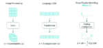
At Mixed-Signal Devices, we’re reinventing timing for the modern world. From AI data centers to radar, 5G base stations to aerospace systems, today’s technologies demand timing solutions that are not only ultra-fast but also programmable, scalable, and rock-solid under extreme conditions. That’s where we come in.

We’re a new kind of timing company, founded by engineers who have built foundational technologies at companies like Broadcom. We saw that conventional clock architectures—especially legacy quartz and analog PLL-based designs—were no longer scaling with system demands. We created something different: a digitally synthesized, CMOS-based timing platform that combines the precision of crystals with the flexibility of digital design.

Our patented “Virtual Crystal” architecture enables multi-gigahertz performance with femtosecond-level jitter and sub-Hz frequency programmability. It’s all built on silicon, optimized for integration, and designed to simplify clock architectures from day one.

What problems are you solving?

Modern electronic systems are running faster, hotter, and more complex than ever. Whether you’re trying to scale a GPU fabric in an AI data center or coordinate coherent RF signals in a phased array radar, timing precision becomes the bottleneck. Traditional clocking solutions weren’t built for this world.

We solve that by eliminating the analog limitations. Our all-CMOS digital synthesis platform delivers low-jitter, low-phase-noise clocks at up to 2 GHz, without bulky crystals or noisy PLLs. And because we built our own DAC architecture and waveform engine, we’ve eliminated the spurs and drift that plague conventional solutions.

Whether it’s deterministic synchronization across a rack, reference clock cleanup for PCIe or SerDes, or generating clean LOs for high-speed converters, our portfolio is built to meet the needs of engineers building the world’s most advanced systems.

What are your strongest application areas?

We’re seeing strong traction in four key segments:

  1. AI Infrastructure – Our clocks and synthesizers support ultra-low jitter and precise synchronization for GPU/CPU boards, optical modules, SmartNICs, and PCIe networks.
  2. Wireless Infrastructure and 5G/6G – Our jitter attenuators and oscillators provide reference cleanup and deterministic timing for fronthaul/midhaul networks.
  3. Defense and Radar – Our RF synthesizers with phase-coherent outputs are ideal for beamforming, MIMO, and SAR systems.
  4. Test & Measurement / Instrumentation – Engineers love our digitally programmable, wideband signal sources for high-speed converter testing and system prototyping.
What keeps your customers up at night?

They’re building faster systems with tighter timing and synchronization margins—and legacy clocking just isn’t cutting it. As Ethernet speeds scale to 800G and 1.6T, and new modulation schemes like PAM6 and PAM8 take hold, they’re running into noise, jitter, and skew problems that conventional architectures can’t overcome.

They also worry about integration and supply chain predictability. We address both by delivering clock products that are smaller, programmable, and available in standard CMOS packages. That means fewer components, easier integration, and better reliability—even across temperature and voltage swings.

How do you differentiate from other timing companies?

Mixed-Signal Devices is the first company to combine the best of digital synthesis, high-performance DACs, and BAW-based timestamping into a single, scalable clocking platform. Our “Virtual Crystal” concept gives you phase noise commensurate with high-frequency fundamental mode crystals, crystal-like stability, but with digital programmability and sub-Hz resolution. And our femtosecond jitter performance rivals—and in many cases exceeds—the best quartz and PLL-based solutions.

We’re not retrofitting old designs. We built our architecture from the ground up to meet modern demands. That means our products are clean, simple, and powerful—ideal for engineers who don’t want to patch together three chips when one will do.

What new products are you most excited about?

We just launched the MS4022 RF Synthesizer, a digitally programmable wideband source with output up to 22 GHz and jitter as low as 25 fs RMS. It’s phase-coherent, and can lock to anything from a 1 PPS GPSDO to a 750 MHz reference. It’s a game-changer for radar, wireless, and test equipment.

We’ve also introduced the MS1130 and MS1150 oscillators and MS1500/MS1510 jitter attenuators, supporting frequencies up to 2 GHz and jitter as low as 19 fs. These are already being evaluated in AI compute fabrics and 5G radio access networks. Everything is built on our same core architecture—clean signals, robust programmability, and compact form factors.

How do customers typically engage with your company?

We work closely with design teams, often from first concept through final product. Our solutions are used by some of the most advanced engineers in radar, compute, networking, and defense, and they’re looking for a partner who understands both the signal chain and the system-level challenges.

We also work through select distributors and field engineers, so customers can get hands-on support quickly and scale into volume smoothly. Whether it’s early-stage sampling or joint product validation, we aim to be a true technical partner, not just a vendor.

How do you see timing evolving, and what role will Mixed-Signal Devices play?

Timing is becoming the next system bottleneck. As systems scale to higher speeds (for example 1.6T networking), timing solutions must become faster, cleaner, and more deterministic. Legacy analog solutions can’t keep up. Mixed-Signal Devices is creating a new category of timing, one that’s digital at its core, programmable by design, and scalable with Moore’s Law. We believe the future of timing is fully synthesized, digitally defined, and built to unlock the next generation of compute, communications, and autonomy. That’s the future we’re building, and we’re just getting started.

Also Read:

CEO Interview with Andrew Skafel of Edgewater Wireless

CEO Interview with Jutta Meier of IQE

Executive Interview with Ryan W. Parker of Phononic Inc.


AI’s Transformative Role in Semiconductor Design and Sustainability

AI’s Transformative Role in Semiconductor Design and Sustainability
by Admin on 08-02-2025 at 6:00 pm

On July 18, 2025, Serge Nicoleau from STMicroelectronics delivered a compelling presentation at DACtv, as seen in the YouTube video exploring how artificial intelligence (AI) is revolutionizing semiconductor design, edge computing, and sustainability. Addressing a diverse audience, Serge highlighted AI’s pervasive integration across industries and its critical role in enhancing R&D processes, optimizing edge devices, and addressing global challenges like climate change through innovative chip design.

Serge began by illustrating AI’s ubiquity, from autonomous vehicles navigating San Francisco streets to NASA’s Mars rovers and AI-driven non-player characters in gaming. These applications, enabled by semiconductor advancements, mimic human capabilities like sensing, acting, connecting, and processing. Sensors (e.g., accelerometers, gyroscopes) and actuators bridge the physical and digital worlds, with microcontrollers (MCUs) and microprocessors (MPUs) processing data either locally or in data centers. AI augments this bridge by learning from data in the cloud and deploying trained algorithms at the edge, where data is generated, enhancing efficiency and responsiveness.

The computing pyramid, as Serge described, illustrates the scale of AI deployment: thousands of data centers, millions of edge gateways, and billions of tiny edge devices. Edge AI, particularly in microelectromechanical systems (MEMS), is pivotal. For instance, a six-axis inertial measurement unit (IMU) with an embedded digital signal core runs machine learning algorithms to manage system wake-up intelligently, preserving battery life in wearables. More complex intelligent sensor processing units (ISPUs) integrate multiple chips in a single package, enabling sophisticated AI algorithms for tasks like anomaly detection, crucial for IoT and automotive applications.

In semiconductor design, AI accelerates R&D by streamlining analog and digital design flows. Analog design, traditionally labor-intensive, benefits from AI-driven automation in schematic creation and layout optimization, reducing design time. Digital design leverages AI for tasks like power estimation and verification, enhancing efficiency. Serge emphasized STMicroelectronics’ AI-powered eco-design approach, which includes a comprehensive checklist to ensure sustainable products. This involves reducing power consumption, minimizing manufacturing footprints, enabling green technologies (e.g., efficient wind or solar farms), and prioritizing human well-being through applications like healthcare wearables.

Sustainability is a core focus, with AI enabling chips that optimize energy use and support ecological technologies. For example, AI-driven sensors in smart grids enhance energy efficiency, while edge devices reduce data transmission to the cloud, lowering carbon footprints. Serge underscored the semiconductor industry’s role in combating climate change, noting that innovative chip architectures are essential for sustainable solutions.

Addressing an audience question from a UIC researcher about AI in academic chip prototyping with limited resources, Serge drew parallels with healthcare, where 25% of new molecules are AI-selected. He suggested federated learning as a solution, where local models are trained on sensitive or limited datasets (e.g., chip design points or synthetic data) without sharing raw data, protecting intellectual property. These models are aggregated at a higher level to enhance performance, enabling academia to leverage collective data while maintaining privacy. This approach, gaining traction in healthcare, could revolutionize semiconductor research by pooling resources across institutions.

Serge concluded by emphasizing AI’s omnipresence, likening it to personal assistants like Alexa or Siri, and its critical role in edge and data center computing. The semiconductor industry, he argued, is at the heart of this transformation, driving novel chip architectures and sustainable practices. As AI proliferates, it demands collaborative innovation to address data privacy, computational constraints, and environmental challenges, positioning the industry as a key player in shaping a sustainable, AI-driven future.

Also Read:

From Atoms to Tokens: Semiconductor Supply Chain Evolution

The Future of Mobility: Insights from Steve Greenfield

Chip Agent: Revolutionizing Chip Design with Agentic AI


Google Cloud: Optimizing EDA for the Semiconductor Future

Google Cloud: Optimizing EDA for the Semiconductor Future
by Admin on 08-02-2025 at 5:00 pm

On July 9, 2025, a DACtv session featured a Google product manager discussing the strategic importance of electronic design automation (EDA) and how Google Cloud is optimizing it for the semiconductor industry, as presented in the YouTube video. The talk highlighted Google Cloud’s role in addressing the escalating complexity of chip design, leveraging AI, scalable compute, and collaborative ecosystems to enhance productivity, reduce time-to-market, and support sustainable innovation.

The semiconductor industry faces unprecedented challenges with modern systems-on-chip (SoCs) comprising billions of transistors, driven by demand for AI, 5G, and IoT applications. Traditional on-premises EDA workflows struggle with compute-intensive tasks like simulation, verification, and physical design. Google Cloud’s EDA platform tackles these by offering scalable, high-performance computing (HPC) infrastructure, optimized for hybrid and cloud-native workflows. The speaker emphasized that their platform, built on Google’s robust cloud ecosystem, enables seamless bursting to handle peak workloads, reducing tape-out times by up to 25% for customers, as evidenced by industry case studies.

AI and machine learning (ML) are integral to Google’s EDA strategy. AI-driven tools enhance design optimization, automating tasks like place-and-route, timing analysis, and power estimation. For instance, reinforcement learning algorithms predict optimal layouts, improving power-performance-area (PPA) metrics by 10-15%. The platform integrates Google’s Tensor Processing Units (TPUs) for accelerated ML workloads, enabling faster verification and synthesis. This is critical for AI accelerators, where computational demands are massive, and energy efficiency is paramount to support sustainable data center operations.

The speaker highlighted Google Cloud’s infrastructure-as-code (IaC) capabilities, using tools like Terraform to streamline resource allocation. This ensures flexibility for semiconductor firms, from startups to giants like NVIDIA, to scale compute resources dynamically. The platform supports major EDA tools (e.g., Synopsys, Cadence) and process design kits (PDKs) from foundries like TSMC, ensuring compatibility with existing workflows. Security features, including enterprise-grade encryption, protect sensitive IP, addressing concerns in automotive and defense applications.

Sustainability was a key focus, with AI data centers consuming gigawatts of power. Google Cloud’s EDA solutions optimize chip designs for energy efficiency, reducing power consumption in edge devices and data centers. For example, AI-driven power modeling in chiplet-based designs cuts energy use by up to 20%, aligning with industry goals to minimize environmental impact. The speaker noted Google’s commitment to carbon-neutral operations, encouraging designers to leverage their platform for greener chip solutions.

The session also emphasized community collaboration. Google’s Advanced Computing Community series, accessible via QR codes shared during the talk, fosters industry-wide partnerships. These initiatives include webinars, workshops, and forums where EDA vendors, foundries, and designers collaborate to advance tools and methodologies. The speaker invited attendees to engage with Google experts at their booth or colleagues like Anand and Push for ongoing discussions, underscoring a collaborative approach to innovation.

An audience question on integrating AI with limited datasets was addressed by referencing federated learning, enabling secure data sharing across organizations. This approach, inspired by healthcare, supports academic and smaller firms in leveraging AI without compromising IP. The session concluded with a call to join Google’s journey in transforming EDA, ensuring the semiconductor industry meets the demands of an AI-driven future while prioritizing efficiency and sustainability.

Also Read:

Synopsys FlexEDA: Revolutionizing Chip Design with Cloud and Pay-Per-Use

Perforce and Siemens: A Strategic Partnership for Digital Threads in EDA

AI-Driven Chip Design: Navigating the Future


Synopsys FlexEDA: Revolutionizing Chip Design with Cloud and Pay-Per-Use

Synopsys FlexEDA: Revolutionizing Chip Design with Cloud and Pay-Per-Use
by Admin on 08-02-2025 at 4:00 pm

On July 9, 2025, Vikram Bhatia, head of product management for Synopsys’ cloud platform, and Sashi Obilisetty, his R&D engineering counterpart, presented a DACtv session on Synopsys FlexEDA, as seen in the YouTube video. Drawing from three and a half years of data, the session showcased how this cloud-based, pay-per-use EDA platform has slashed tape-out times by months, offering scalable, cost-efficient solutions for the semiconductor industry’s escalating design challenges.

FlexEDA addresses the growing complexity of modern chip designs, with systems-on-chip (SoCs) now featuring billions of transistors. Traditional EDA workflows, constrained by on-premises infrastructure, struggle with compute-intensive tasks like simulation, verification, and physical design. FlexEDA leverages cloud scalability to provide on-demand compute resources, enabling companies to burst workloads during peak design phases. Bhatia highlighted that customers, ranging from startups to tier-one semiconductor firms, have reduced tape-out schedules by several months, with some achieving up to 30% faster design cycles through FlexEDA’s elastic compute capabilities.

The platform’s pay-per-use model is a game-changer, particularly for batch-oriented tools like VCS, PrimeTime, PrimeLib, PrimeSim, and StarRC. Unlike traditional per-user licensing, which often underutilizes interactive tools with GUIs, FlexEDA charges based on actual usage, measured precisely for compute-heavy batch jobs. This ensures cost neutrality, as Bhatia emphasized, aligning expenses with project needs. For example, running hundreds or thousands of licenses for verification or timing analysis becomes affordable, as customers only pay for resources consumed. This model optimizes engineering budgets and time, especially for smaller firms with limited capital.

Sashi detailed the technical underpinnings, noting FlexEDA’s integration with cloud-native infrastructure. The platform supports hybrid workflows, seamlessly connecting on-premises systems with cloud resources via tools like Synopsys’ Design Compiler and Fusion Compiler. AI and machine learning enhance FlexEDA’s capabilities, optimizing tasks like place-and-route and power analysis. For instance, AI-driven algorithms predict optimal design configurations, reducing iterations and improving power-performance-area (PPA) metrics by 10-15%. The platform’s robustness stems from extensive testing and customer data, ensuring reliability across diverse workloads, from AI accelerators to automotive chips.

Addressing an audience question on cost management, Bhatia clarified that FlexEDA’s pricing is designed to be neutral, avoiding overcharges while ensuring Synopsys remains financially sustainable. Only flagship tools suited for batch processing are included in the pay-per-use model, as converting interactive tools is engineering-intensive and less scalable. This strategic focus maximizes ROI for customers running high-volume simulations, a critical need as chip complexity grows with AI and 5G applications.

The session underscored broader industry trends. With the semiconductor market projected to hit $1 trillion by 2030, tools like FlexEDA are vital for managing complexity and meeting time-to-market demands. The cloud model mitigates compute shortages, a bottleneck for traditional workflows, while supporting sustainability by optimizing resource use. Bhatia invited attendees to explore details at synopsys.com/cloud, emphasizing the platform’s role in driving innovation.

FlexEDA’s success reflects a shift toward cloud-native EDA, enabling scalable, efficient, and cost-effective design processes. By leveraging cloud infrastructure and AI, Synopsys empowers designers to tackle modern challenges, ensuring the industry remains agile in an AI-driven era. The session concluded with a call to join the next DAC exhibitor forum, signaling Synopsys’ commitment to advancing chip design innovation.

Also Read:

Perforce and Siemens: A Strategic Partnership for Digital Threads in EDA

AI-Driven Chip Design: Navigating the Future

IBM Cloud: Enabling World-Class EDA Workflows