Bronco Webinar 800x100 1

Mask and Optical Models–Evolution of Lithography Process Models, Part IV

Mask and Optical Models–Evolution of Lithography Process Models, Part IV
by Beth Martin on 10-10-2011 at 4:50 pm

Will Rogers said that an economist’s guess is liable to be as good as anyone’s, but with advanced-node optical lithography, I might have to disagree. Unlike the fickle economy, the distorting effects of the mask and lithographic system are ruled by physics, and so can be modeled.

In this installment, I’ll talk about two critical components of process models: mask models and optical models. Mask models come in two different flavors: those related to the 1D and 2D geometries on the mask and those related to 3D effects. Optical models are fundamental to representing the lithography imaging sequence, and have a well-established simulation methodology.

Mask Models

Historically, OPC models were calibrated based on an assumed exact match of the physical test mask and the test pattern layouts representing the test mask. However, the mask patterning process exhibits systematic proximity effects such as corner rounding and isolated-to-dense bias. In the past, it was acceptable to lump the systematic mask proximity effects into the resist process model because the mask manufacturing process is usually invariant for the life of the wafer technology. This means, however, that anytime the mask process changes substantially, the OPC model has to be recalibrated.

More significantly, the OPC model incorrectly ascribes mask behavior to the photoresist model, which limits the predictability of the model. Recent work on mask process proximity modeling is changing this (Tejnil 2008; Lin 2009; Lin 2011). This work involves calibrating a mask process model (MPC) based on mask CD or contour measurements, then referencing the MPC model to describe the mask input to the wafer OPC calibration flow. A 50% reduction in mask CD variability can be realized with this approach.

Mask models have also evolved to account for the introduction of alternating phase shift masking (PSM) into manufacturing, which raised awareness of the impact of mask topography on wafer lithography. Ultimately this aggressive PSM approach was replaced with more manufacturable solutions, including attenuated-PSM, which eliminated etched quartz in favor of a thin, partially absorbing layer.

The extensively used Kirchhoff, or flat mask approximation, assumes that the mask is sufficiently thin that the diffracted light is computed by means of scalar or vector diffraction theory. This is in contrast to rigorous electromagnetic field (EMF) simulation, which accounts explicitly for the topography and refractive indices of the mask materials, and solves Maxwell’s equations in 3D (a highly compute intensive operation not suitable for full-chip).


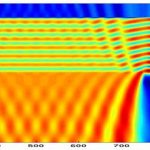
Figure showing near field intensity calculated by rigorous 3D electromagnetic field simulation.

There are many approximation methods that enable a reduction of this 3D EMF system to simpler 1D or 2D representations. Comparison to full rigorous simulation shows an advantage in accuracy by accounting for 3D mask effects versus the Kirchhoff mask, but in practice, the process model can easily adapt to effectively account for the same CD behavior. This is analogous to the mask CD effect described above. Recently, even thinner absorbing layers have been reported, which further reduce the mask 3D contribution to wafer CD variation, thus rendering the continued use of the Kirchhoff approximation a reasonable trade-off.

3D mask effects are sensitive to the angle of incidence of the light impinging upon the mask, and for high NA systems, it is necessary to account for this effect. Approximation methods are available that effectively sectorize the source then calculate the mask signal corresponding to each sector. These approaches deliver accuracy within a few nm of the rigorous simulation result.

Optical Models

Optical models represent the lithography imaging sequence. As introduced above, full chip simulations commonly employ the SOCS (sum of coherent systems) approximation to represent the intensity as a sum of convolutions of the mask m with k different optical kernels f[SUB]n[/SUB], as described in Equation 1.

(Equation 1)

For optical models, there is a strong linear dependence of simulation time on the number of SOCS decomposition kernels used in the simulation. In addition, there is a quadratic dependence on the optical diameter associated with the model. The magnitude of the eigen value coefficients ɸ[SUB]n[/SUB] in Equation 1 decay quickly as n increases. So in practice, as a compromise between accuracy and runtime, it is often the case that 100 or fewer optical kernels are used with an OD < 2.0 μm.

There are many exposure-related factors influencing wafer CDs which can be represented in the simulation. These include wavelength, numerical aperture, ambient refractive index, film stack optical properties, exposure dose and focus, focus blur (induced by stage tilt, stage synchronization errors, or laser bandwidth), illumination intensity and polarization, pellicle thickness, and projection optics aberrations. The model parameters associated with these factors can be input as known values or can be optimized over a user-input range during calibration. Care must be taken, however, in allowing these parameters to move too far from their design values, as this may result in a less physical model. Exposure dose and focus are adjusted in the simulator to empirically match the CD behavior in terms of the scanner dose and focus. A Jones Matrix representation of the entire optical system, or alternatively individual Zernike coefficients for system aberrations can be input into the simulator directly.

It is well known that the optical proximity effect is highly dependent upon the illumination profile, and that the actual profile differs from the profile requested by the scanner recipe. Various models have been developed to describe the actual profile analytically, but it is common today to input a symmetrized version of the in-situ measured pupilgram instead of the as-designed version.

The continuous development of mask and optical models that better represent real silicon is crucial to the success (both in technology and economics) of optical lithography in upcoming process nodes. In the next installment of this series, I will discuss the semi-emperical resist and etch models used for full-chip correction and verification.

— John Sturtevant

To read the full technical paper on this topic, download Challenges for Patterning Process Models Applied to Large Scale.
Want to read past installments of this series? Part I, Part II, Part III



Solido & TSMC Variation Webinar for Optimal Yield in Memory, Analog, Custom Digital Design

Solido & TSMC Variation Webinar for Optimal Yield in Memory, Analog, Custom Digital Design
by Daniel Nenni on 10-09-2011 at 4:01 pm

Solido has announced webinars for North America, Europe and Asia on October 12-13. They will be describing the variation analysis and design solutions in the TSMC AMS Reference Flow 2.0 announced at the Design Automation Conference this year.

“We are pleased to broaden our collaboration with Solido in developing advanced variation and design methodology in AMS Reference Flow 2.0. TSMC customers can use Solido Variation Designer with TSMC 28nm process technology to achieve better product quality in their AMS designs.” Suk Lee, Director of Design Infrastructure Marketing, TSMC.


Variation effects are critical to consider for designers working on nanometer designs, impacting the design’s electrical characteristics. In a recent survey, variation-aware custom IC design was ranked the #1 area requiring advancement over the next two years. The survey showed 53% of design groups missed deadlines or experienced re-spins due to variation issues, designers experienced an average 2 month delay due to variation issues, and designers spent an average 22% of design time on variation issues.


Solido Variation Designer products were selected for TSMC’s Advanced PVT and Advanced Monte Carlo sub flows. Solido products work with TSMC process and device models, improving design performance, power and area, maximizing parametric yield and avoiding re-spins and project delays.


The webinar will be presented by Nigel Bleasdale, Director of Product Management at Solido and Jason Chen, Design Methodology and Service Marketing at TSMC. Topics covered will be:

[LIST=1]

  • Variation challenges in custom IC design
  • Variation-aware solutions available in the TSMC AMS reference flow
  • Methods to develop and verify designs over PVT corners in less time
  • How to efficiently apply Monte Carlo techniques in design sign-off
  • How Monte Carlo is really possible up to 6-sigma
  • Customer case studies of the above methods

    Register here (www.solidodesign.com/page/tsmc-solido-webinar/) for a 1 hour webinar:
    North America: Wed October 12, 2011 – 10am PDT
    Europe: Wed October 12, 2011 – 2pm BST/3pm CET
    Taiwan: Thurs October 13, 2011 – 9am CST
    Japan: Thurs October 13, 2011 – 10am JST
    Korea: Thurs October 13, 2011 – 10am KST


  • How ST-Ericsson Improved DFM Closure using SmartFill

    How ST-Ericsson Improved DFM Closure using SmartFill
    by Daniel Payne on 10-07-2011 at 2:38 pm

    DFM closure is a growing issue these days even at the 45nm node, and IC designers at ST-Ericsson have learned that transitioning from dummy fill to SmartFill has saved them time and improved their DFM score.

    The SOC
    ST-Ericsson designed an SOC for mobile platforms called the U8500 and their foundry choice was a 45nm node at STMicroelectronics.

    They called the chip U8500 and it had to balance battery life, graphics and a multitude of competitive features. This SOC includes:

    • Single-chip base band and APE
    • HSPA+ Modem Release 7
    • SMP Dual ARM Cortex A9 1GHz multicore processor
    • Symbian foundation, Linux Android, MeeGo and Windows Mobile OS support
    • High-definition 1080p camcorder and video
    • About 100 hours audio playback
    • 10 hours HD video playback
    • TV out using HDMI
    • Video and imaging accelerators

    Low power goals were achieved by using:

    • Adaptive Voltage Scaling
    • Dynamic voltage and frequency Scaling
    • CPU Wait for Interrupts (WFI)
    • RAM data retention during WFI
    • Fast wake-up
    • Lower power IO: HDMI, MIPI, LP DDR2, USB

    DFM Closure

    The fab (STMicroelectronics) at first provided standard DummyFill rules in their Calibre deck to ST-Ericsson. The result was that DummyFill didn’t meet all of the density related constraints in their process. There were two density rules not being satisfied with the DummyFill approach (fill first, verify after fill is completed).

    Dummy fill example where extra shapes are added to an IC layer in order to meet layout density requirements.

    The second approach was to tweak the dummy fill rule deck in order to reach a DFM clean layout. Even this approach was not a complete success as shown in the following comparison table:

    The final results in the third row of the comparison table show that using the new SmartFill capability in The Calibre YieldEnhancer tool produced a layout with 0 DRC errors and the lowest DFM score.

    DummyFill adds new fill shapes across the entire chip first, then you have to run a DRC tool as a second step to see your DRC and DFM score results.

    In contrast the SmartFill approach is analyzing the new fill shapes as they are being placed to make sure that they are DRC clean while meeting the fill constraints. To the EDA tool user it has now become more of a push-button approach instead of an iterative approach, you just need to make sure that your foundry process is supporting Caliber YieldEnhancer.

    The U8500 SOC has 1.2 million standard cells at the top level along with 32Mbit of SRAM, so saving time in DFM closure really helped out.

    Fill and Timing
    Because SmartFill (or DummyFill) adds new shapes to layers the timing of an IC will be impacted. A new fill shape adds extra parasitic capacitance which in turn can impact timing results.

    STMicroelectronics ran a digital test chip in their 45nm process to make some comparison measurements of the DummyFill versus SmartFill options:

    With SmartFill the table shows that the run time is close to that of DummyFill, while the GDS size got smaller, more fill shapes were created, total filled area was reduced, no DRC errors reported and the capacitance values were actually reduced.

    The “purpose tile_O” shapes are the largest fill shapes and they have a higher spacing requirement between the layout and these fill shapes. Fewer of these shapes is an improvement because it creates less OPC work and helps to reduce capacitance values, which in turn means less impact on timing.

    Design teams typically only re-run timing on their most critical paths after SmartFill, not re-run all static and dynamic testing.

    With Calibre YieldEnhancer you can even provide a list of critical nets as an input so that SmartFill can avoid changing your timing on these nets during the fill process.

    Rapid Thermal Annealing (RTA)
    During semiconductor manufacturing there are thermal steps used to create shallow junctions which then affect transistor performance like: Vth (Threshold Voltage) shifts, Vth variation. The three things that contribute to RTA effects are: pattern density of the layout, the RTA temperature, and the amount of time spent in annealing. As a designer we can only impact the pattern density of the layout.

    Fill shapes created by Calibre SmartFill take this into account and control the reflectivity of the wafer surface. This helps to control the electrical variability introduced by RTA.

    Summary
    To ensure DFM closure, maintain timing integrity and reduce variability effects at the 45nm node you should consider moving from the DummyFill approach to a SmartFill approach. ST-Ericsson and STMicroelectronics have achieved a better DFM score by using Calibre SmartFill on their U8500 SOC. More details about this topic can be found in this white paper.


    Jasper User Group Meeting

    Jasper User Group Meeting
    by Paul McLellan on 10-07-2011 at 11:59 am

    Jasper’s Annual User Group Meeting is on November 9th and 10th, in Cupertino California. It will feature users from all over the world sharing the best practices in verification. If you are a user of Jasper’s products then you should definitely plan to attend. This year there is so much good material that the meeting is two days long.

    Of course there will be many presentations by Jasper themselves. But much of the meeting will be taken up with users presenting their own experiences. If you are a Jasper customer and are interested in proposing a presentation, then contact Rob van Blommestein at robvb@jasper-da.com.

    The full agenda is still being developed, but already there are user presentations on:

    • Simulation task reduction
    • RTL verification
    • X-propagation
    • Using formal to verify real CPUs
    • RTL sequential equivalence checking
    • Micro-architecture validation
    • SoC integration
    • Macro verification
    • RTL Development
    • Post-silicon debug

    and presentations by Jasper on:

    • Product roadmap
    • Hints and tips for using Jasper solutions more effectively
    • Architecture validation
    • Creating verification IP
    • Introduction to intelligent proof kits
    • Property synthesis

    To find out more about the meeting, or to register for the event, go here.


    Testing, testing… 3D ICs

    Testing, testing… 3D ICs
    by Beth Martin on 10-06-2011 at 7:01 pm

    3D ICs complicate silicon testing, but solutions exist now to many of the key challenges. – by Stephen Pateras

    The next phase of semiconductor designs will see the adoption of 3D IC packages, vertical stacks of multiple bare die connected directly though the silicon. Through-silicon vias (TSV) result in shorter and thinner connections that can be distributed across the die. TSVs reduce package size and power consumption, while increasing performance due to the improved physical characteristics of the very small TSV connections compared to the much larger bond wires used in traditional packaging. But TSVs complicate the test process, and there is no time to waste in finding solutions. Applications involving the stacking of one or more memory die on top of a logic die, for example using the JEDEC Wide IO standard bus interface, are ramping quickly.

    One key challenge is how to test the TSV connections between the stacked memory and logic die. There is generally no external access to TSVs, making the use of automatic test equipment difficult if not impossible. Functional test (for example, where an embedded processor is used to apply functional patterns to the memory bus) is possible but is also slow, lacks test coverage, and offes little to no diagnostics. Therefore, ensuring that 3D ICs can be economically produced calls for new test approaches.

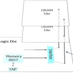
    A new embedded test method that works for test and diagnostics of memory on logic TSVs is built on the Built-In Self-Test (BIST) approach that is already commonly used to test embedded memories within SoCs. For 3D test, a BIST engine is integrated into the logic die and communicates to the TSV-based memory bus that connects the logic die to the memory as illustrated in Figure 1.

    For this solution to work, two critical advances over existing embedded memory BIST solutions were necessary.

    One is an architecture that allows the BIST engine to communicate to a memory bus rather than directly to individual memories. This is necessary partly because multiple memories may be stacked within the 3D IC, but mostly to allow the BIST engine to test the memory bus itself, and hence the TSV connections, rather than just the memories. Test algorithms tailored to cover bus-related failures are used to ensure maximum coverage and minimal test time. Because of this directed testing of the memory bus, the 3D BIST engine can also report the location of failures within the bus, which allows diagnosis of TSV defects.

    The second critical advance in this new 3D BIST solution is that it is run-time programmable. Using only the standard IEEE 1149.1 JTAG test interface, the BIST engine can be programmed in silicon for different memory counts, types, and sizes. Because the BIST engine is embedded into the logic die and can’t be physically modified without a design re-spin, this adaptability is essential. With full programmability, no re-design is needed over time even as the logic die is stacked with different memories and memory configurations for different applications.

    An automated flow is available for programming the BIST engine (for wafer or final package testing) to apply different memory test algorithms, to use different memory read/write protocols, and to test different memory bus widths and memory address ranges. The patterns needed to program the engine through the JTAG interface pins are generated in common formats, such as WGL or STIL, to be loaded and applied by standard automatic test equipment.

    Because this 3D test solution is embedded, it needed to have minimal impact on design flows and schedules and no impact on design performance. This is done through an automated RTL flow that integrates the BIST engine into the logic die and fully verifies its operation. The flow is compatible with all standard silicon design flows and methodologies. There is no impact to design performance because the BIST engine intercepts the memory bus with multiplexing logic placed at a point in the functional path with sufficient slack.

    This new embedded solution for testing TSVs between memory and logic die is cost effective, giving the best balance between test time and test quality. Engineers considering designing in 3D need to feel confident that they can test the TSVs without excessive delay or risk. This solution shows how that can be achieved and opens the way for a more rapid adoption of 3D design techniques.

    Stephen Pateras is product marketing director for Mentor Graphics Silicon Test products.

    The approach described above forms part of the functionality of the Mentor Graphics Tessent[SUP]®[/SUP]MemoryBIST product. To learn more, download the whitepaper 3D-IC Testing with the Mentor Graphics Tessent Platform.


    Circuit Simulation and Ultra low-power IC Design at Toumaz

    Circuit Simulation and Ultra low-power IC Design at Toumaz
    by Daniel Payne on 10-06-2011 at 4:31 pm

    I read about how Toumaz used the Analog Fast SPICE (AFS) tool from BDA and it sounded interesting so I setup a Skype call with Alan Wong in the UK last month to find out how they design their ultra low-power IC chips.


    Interview

    Q: Tell me about your IC design background.
    A: I’ve been at Toumaz almost 8 years now and before that at Sony Semi for 5.5 years. My IC design experience goes back to 1997, then starting in 2005 I’ve been in the IC design group for wireless.

    Q: Does Toumaz have a CAD group?
    A: Yes, we do have two CAD engineers.

    Q: What EDA tools are you using?
    A: For RTL simulation we have Mentor Questa, and on physical verification we’re using Calibre. Place & Route it’s Synopsys and for IC layout we’ve got Cadence Virtuoso and Assura (verification). Circuit simulation we have the Analog Fast SPICE tool from Berkeley Design Automation.

    Q: How about your product life cycle?
    A: Most of our IC designs go from definition to Tape out in about 18 months, some are quicker. Foundry choices have been: TSMC, IBM, Infineon, UMC.

    Q: What’s the first thing that you do when silicon comes back from the fab?
    A: With our engineering samples we first test to see if our spec is met, then we start to characterize with initial functional vectors plus the specialized analog RF testing.

    Q: For circuit simulation tools, what have you used before?
    A: We’ve used Cadence Spectre tools before, then we switched over to BDA. We found better results with the Berkeley tool in terms of speed. In our evaluation we used internal designs, multiple test benches and clock circuits, taking several weeks to complete our benchmarking. Overall we saw, about 5X quicker with AFS.

    Q: When the foundry provides SPICE models have there been any issues?
    Q: Yes, we had some issues with model cards and BDA. There were some differences between Spectre and BDA, causing BDA to make some tweaks in their BSIM4 RF models.

    Q: How do you simulate the whole mixed-signal chip?
    A: For Mixed-signal chips we model at two levels of abstraction, behavioral and transistor level. During simulation we can swap out transistor level versus behavioral to get the speed and accuracy trade-off we need. For analog blocks we simulate at the transistor level.

    Q: Why not use a Fast SPICE simulator for full-chip circuit simulation?
    A: Our experience shows that Full-chip with Fast SPICE gives fast but wrong answers.

    Q: Which process nodes are you designing at?
    A: Quite a range: 130nm and 110nm, some 65nm nodes.

    Q: How large are your design teams?
    A: Our design team for an SOC uses a Personal Area Network and has some layout designers, firmware team, test and production engineers, maybe 20 people in total.

    Q: What is your version control system?
    A: We have used SVN for just the RTL coding side and also tried the Design Management Framework within Cadence IC 5. Our plan is to start using ClioSoft soon in Cadence IC 6.

    Q: Are there other circuit simulation tools that you’ve looked at?
    A: Quite a few: Synopsys, Aglient and Golden Gate.

    Q: What’s really important for your circuit simulations?
    A: Accuracy and the ability to do long simulation runs, some are up to one week in duration. We do some top level parametric simulation, try different scenarios, and run lots of configurations.

    Q: What needs improvement for your circuit simulation?
    A: Well, there’s some room for improvement with co-simulation, it can be a bit flakey. We co-simulate with Verilog.

    Q: How often does BDA update their software?
    A: With BDA there are updates every few months, so we just wait for the new features that we need then install it about once a quarter.

    Q: What about your layout tools from Cadence?
    A: We freeze the Cadence toolset at the start of each project and update tools only if really needed during a project.

    Q: What was the learning curve for the BDA circuit simulator?
    A: The learning curve was short for us, we now know how to setup the options to get the accuracy vs speed.

    Q: What’s your wish list for BDA?
    A: I would prefer more flexible license terms throughout the year (like Cadence credits). We always want circuit simulation to be Faster, more accurate, and improved DC convergence.

    Summary
    Toumaz uses a mixture of EDA tools to design their ultra low-power IC designs, working with vendors like: Berkeley Design Automation, Cadence, Mentor Graphics, Synopsys and ClioSoft.


    SuperSpeed USB finally take off! Synopsys claim over 40 USB 3.0 IP sales…

    SuperSpeed USB finally take off! Synopsys claim over 40 USB 3.0 IP sales…
    by Eric Esteve on 10-06-2011 at 9:06 am

    SuperSpeed USB specification was released in November 2008! Even if we can see USB 3.0 powered peripherals shipping now, essentially external HDD, connected to PC equipped with Host Bus Adaptors (as PC chipset from Intel or AMD were not supporting USB 3.0), it will take up to the second quarter of 2012 before PC will be shipped with “native” USB 3.0 support; native just means that PC chipset will integrate SuperSpeed USB. This will be the key enabler for USB 3.0 wide adoption in PC & Media Tablet, Smartphone and many consumer electonic applications.

    It will have taken more than three years to Intel –and AMD- to finally support USB 3.0 technology. If we trust InStat, it will only take two years before more than 90% of PC being shipped natively support this technology, see the figure:

    This short reminder to help the reader understand the importance of Synopsys’s Press Release about the explosion of the Design-in for SuperSpeed USB IP. Synopsys USB Marketing manager Eric Huang is claiming 40 sales since USB 3.0 IP product launch, in 2009, and we think, first that this is true, and second that 25 sales have been made in 2011 only.

    Some more history: Synopsys was already the USB IP market leader with more than 60% market share when they bought ChipIdea from MIPS, to get a more than 80% market share at the time where the USB IP market was only made of High Speed (2.0), Full Speed and Low Speed. When SuperSpeed USB was released, the backward compatibility constraint imposes to provide both USB 2.0 and USB 3.0 function to be 100% compatible. IP vendors previously active in the USB 2.0 market had disappear (except Faraday) and the new comers, able to easily manage the design of a 5 Gbps SerDes to build the USB 3.0 PHY were missing the “stupid” 480 Mbps PHY you need to provide in order to be fully compatible…

    Then Synopsys has been in a very good position to capitalize on the existing USB port-folio and experience, develop SuperSpeed USB PHY and Controller and integrate all the pieces to build a complete, 100% USB 3.0 compatible solution. The testimonial from Realtek highlights how important was Synopsys’s track record in USB 2.0 to support their selection for USB 3.0:

    “We taped-out Synopsys’ DesignWare USB 3.0 host and USB 3.0 device in three chips targeted at the digital home and PC peripheral markets, and all are now shipping in mass production,” said Jessy Chen, executive vice president of Realtek Semiconductor Corporation. “We chose Synopsys DesignWare IP because of the company’s excellent track record in USB 2.0. With Synopsys’ USB 3.0 IP now fully certified and proven in our chips, we are certain we picked the right IP partner. We have been at the forefront of USB 3.0 development and integration, and have many innovative chips using Synopsys USB 3.0 IP coming in 2012.”

    Very important for today’ SoC designs is the capability offered by the IP vendor to support the validation: of the function (IP), of the chip prior to mask generation and of the Software as early as possible in the product development cycle, to speed-up Time-To-Market and guarantee first pass success. This is possible when the following boxes are ticked:

    • Verification IP available at the same time than the IP
    • Especially important for a standard based protocol, IP certification obtained
    • In order to validate the Software as early as possible, in parallel with the SoC development, availability of FPGA-based prototype solution, HAPS, as stated by DisplayLink:

    “Working with Synopsys for our USB 3.0 controller, HDMI controller and PHY IP helped us mitigate our project risk and reach volume production with our first-pass silicon,” said Jonathan Jeacocke, vice president of engineering at DisplayLink. “In addition, we used Synopsys’ HAPS® FPGA-based prototyping solution to build fully functional systems for at-speed testing of USB 3.0 and HDMI, including architecture validation, performance testing, software development and customer demonstrations.”


    Some precision about these HAPS boards:
    · 2 PCs are connected to a HAPS FPGA-based Prototyping platform
    · The HAPS on the left has Synopsys USB 3.0 Host with a Synopsys USB 3.0 PHY daughter card.
    · The HAPS platform on the right has Synopsys USB 3.0 Device, also with the Synopsys USB 3.0 PHY daughter Card.
    · This is also connected via PCIe (using Synopsys PCIe) to a PC running Linux drivers for the Device.

    The HAPS boards and PHY boards are off-the shelf from Synopsys, and the USB 3.0 Host, USB 3.0 Device and PCIe cores are from Synopsys.

    If we look at the market segment where USB 3.0 adoption will come first “In-Stat expects several hundred million USB 3.0-enabled devices will ship in 2012, including a large share of tablets, mobile and desktop PCs, external hard drives and flash drives,” said Brian O’Rourke, research director at In-Stat. “By 2014, we expect many consumer electronics devices to transition to USB 3.0, including digital cameras, mobile phones and digital televisions. Overall, in 2014, we forecast that 1.4 billion USB 3.0 devices will ship. IP suppliers like Synopsys will help fuel this explosion in USB 3.0 adoption.”

    I fully agree with the forecast mentioning several hundred million USB 3.0-enabled devices will ship in 2012, I just would like to precise that external hard drives proposed today to consumers are already USB 3.0-enabled, now in 2011. Moreover, IPNEST don’t think we will have to wait until 2014 to see Smartphone supporting USB 3.0, and we will probably see these devices on the market before, or at the same time than Media Tablet, as more than 60% of Media Tablet are using the same Application processor than Smartphone.

    Then there will be a second wave of consumer electronics devices to transition, namely the Digital TV, Set-Top-Box, Blue Ray Players, to ship in 2012-2013, followed by Digital Video camera and Digital Still cameras. This means IP sales starting now and continuing in 2012 to allow for a minimum development time. In fact we have built a forecast for USB 3.0 IP sales based on a bottom-up analysis, looking at the different application in every market segment which could transition to USB 3.0, and even more important, we have tried to determine when the IP sales will happen, application by application. The result is a very complete 50 pages document, where you can find many useful informations, like the design start evaluation (generating USB 3.0 IP sales) up to 2015:


    Eric Esteve from IPNEST

    – Table of Content for “USB 3.0 IP Forecast 2011-2015” available here


    SoC Realization: Let’s Get Physical!

    SoC Realization: Let’s Get Physical!
    by Paul McLellan on 10-05-2011 at 1:41 pm

    If you ask design groups what the biggest challenges are to getting a chip out on time, then the top two are usually verification, and getting closure after physical design. Not just timing closure, but power and area. One of the big drivers of this is predicting and avoiding excessive routing congestion, which is something that has only downside: area, timing and power are all worse (unless additional metal layers are used which is obviously increases cost).

    A typical SoC today is actually more of an assembly of IP blocks, perhaps with a network-on-chip (NoC) infrastructure to tie it all together, itself an approach partially motivated by better routability aka less routing congestion.

    Some routing congestion, physical congestion, is caused by how the chip floorplan is created. Like playing tic-tac-toe where you always want to start by grabbing the middle square, routing resources in the middle of the chip are at a premium and creating a floorplan that minimizes the number of wires that need to go through there is almost always a good idea. The ideal floorplan, never truly achieved in practice, has roughly even routing congestion across the whole chip.

    But other routing congestion is logical congestion, inherent in the design. This comes in two flavors: core congestion and peripheral congestion.

    Core congestion is inherent in the structure of the IP block. For example, very high fanout muxes will bring a large number of routes into the area of the mux causing congestion. This is inherent in the way the RTL is written and is not something that a good floorplan or a clever router can correct. Other common culprits are high fanout nets, high fanin nets and cells that have a large number of pins in a small area.

    Peripheral congestion is caused when certain IP blocks have large numbers of I/O ports converging on a small number of logic gates. This is not really visible at module development time (because the module has yet to be hooked up to its environment) but becomes so when the block is integrated into the next level up the hierarchy.

    The challenge with logical congestion is that it is baked-in when the RTL is created, but generally RTL tools and groups are not considering congestion. For example, high-level synthesis is focused on hitting a performance/area (and perhaps power) sweet spot. IP development groups don’t know the environment in which their block will be used.

    The traditional solution to this problem has been to ignore it until problems show up in physical design, and then attempt to fix them there. This works fine for physical congestion, but logical congestion really requires changes to the RTL and in ways which are hard to comprehend when down in the guts of place and route. This process can be short-circuited by doing trial layouts during RTL development, but a the RTL must be largely complete for this so it is still late in the design cycle.

    An alternative is to use “rules of thumb” and the production synthesis tool. But these days, synthesis is not a quick push-button process and the rules-of-thumb (high fanout muxes are bad) tend to be very noisy and produce a lot of false positives, structures that are called as bad when they are benign.

    What is required is a tool that can be used during RTL authoring. It needs to have several attributes. Firstly, it needs to give quick feedback during RTL authoring, not later in the design cycle when the authoring teams have moved on. Second, it needs to minimize the number of false errors that cause time to be wasted fixing non-problems. And thirdly, the tool must do a good job of cross-probing, identifying the culprit RTL not just identifying some routing congestion at the gate-level.

    Products are starting to emerge in EDA to address this problem, including SpyGlass Physical, aimed (despite Physical in the name) at RTL authoring. It offers many capabilities to resolve logical congestion issues up-front, has easy to use physical rules and debug capabilities to pin-point roout causes so that they can be fixed early, along iwth simple reports on the congestion status of entire RTL blocks.

    The Atrenta white-paper on SpyGlass Physical can be downloaded here.


    Amazon’s Kindle Fire Spells Trouble for nVidia, Qualcomm and Intel

    Amazon’s Kindle Fire Spells Trouble for nVidia, Qualcomm and Intel
    by Ed McKernan on 10-05-2011 at 11:50 am

    With the introduction of the Kindle Fire, it is now guaranteed that Amazon has the formula down for building the new, high volume mobile platform based on sub $9 processors. In measured fashion, Amazon has moved down Moore’s Law curve from the initial 90nm Freescale processor to what is reported to be TI’s OMAP 4 in order to add the internet, music and movies to its previously single function e-book environment. Some view it as a competitor to Apple, however the near term impact is on brick and mortar competitors (i.e. Barnes and Noble, Walmart etc) and to the mostly snail mail based movie house Netflix.
    Continue reading “Amazon’s Kindle Fire Spells Trouble for nVidia, Qualcomm and Intel”


    AMS Verification: Speed versus Accuracy

    AMS Verification: Speed versus Accuracy
    by Daniel Nenni on 10-03-2011 at 9:16 pm

    I spent Thursday Sept. 22 at the first nanometer Circuit Verification Forum, held at TechMart in Santa Clara. Hosted by Berkeley Design Automation (BDA), the forum was attended by 100+ people, with circuit designers dominating. I spoke with many attendees. They were seeking solutions to the hugely challenging problems they are wrestling with today when verifying high-speed and high-performance analog and mixed-signal circuits on advanced nanometer process geometries.

    Continue reading “AMS Verification: Speed versus Accuracy”