Intro
Mentor, Cadence and Synopsys all offer Verilog simulators, however when was the last time that you benchmarked your simulator against a tool from a smaller company?
I just heard from an RTL designer (who wants to remain anonymous) about his experience comparing a Verilog simulator called CVC from Tachyon against ModelSim from Mentor.
First, let me say that my primary use for the CVC tool is with regard to regressions being done on RTL designs, so it is not a gate level design that I can give you benchmark data on. In my regressions, sometimes the test bench activity contributes as much or more to the total simulation time requirements.
The test case that I was writing about when I first sent you the email was the regression testing for a relatively small digital design of about 150,000 gates in 0.35 micron UMC; however, as I mentioned before, the regressions were being performed on the RTL.
In that design, there are about 7,500 lines of RTL code in the design, and the test bench is about 6,500 lines of RTL code.
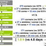
In a regression that took Modelsim Questa 28 hours to complete, CVC completed the work in 10 hours. This regression consists of a bash script that calls the same test bench with different conditions repeatedly to test all the features and automatically verify the performance.
In a more recent test that I have done with a much smaller design, where the test bench takes more time to run than the actual DUT, I ran a 100 msec simulation in 6 minutes with CVC that toom Modelsim Questa over 30 minutes to run. The test bench in this design does a state space model simulation of an analog circuit that is connected to the DUT and performs functional simulation not so much for regression testing, but more for the purpose of design analysis. We do small designs on large geometry due to the power control nature of our business.
In this case, the RTL for the DUT is 12,000 lines and the test bench is 8,000 lines long. As you can see, there are more lines of code here, but the design is about 1/10th the size of the previous example (about 13,000 gates).
We find that the greatest differences in speed between Modelsim Questa and CVC relate to the test bench part; however, we have also noticed that CVC is often 20 to 50 percent faster in the gate level sims as well. Where it does NOT shine is that we run into some trouble using SDF back-annotation with it. We can get it to work, but it seems to be not consistent.
We tend to use CVC more for functional verification and development, but we still use Questa for the back end validation steps.
I know that some of this data is not perhaps as quantitative as the example that you sent to me, but since we have been using CVC now for almost 2 years, I believe that our results have been consistently observed over enough projects such that our group is increasing its use over time due to the speed advantage that it gives us at least in our circumstance.
I have NOT had an opportunity to use it with large designs such as those found in much of the communications, graphics, and other DSP intensive applications where the gate counts get into the millions. So I cannot address that behavior with my current experience with it.